By Nash Reilly | August 8, 2022
Here at River Loop Security, we’re tightly focused on solving hardware security challenges. The nature of our work frequently brings us into contact with problems that:
- deal with intricate technical details of ICs, electrical systems, and products
- are, by their very nature, technically risky - we frequently run across challenges with no known solutions, and, as such, we have to try out technical approaches that can only be verified experimentally.
These two factors mean that we end up designing and fabricating a lot of circuit boards. It’s often the fastest way to quickly prove out hardware security techniques. We’ve come to find that traditional turnkey circuit board manufacturing is both too expensive and, crucially, too slow to meet our needs. Over the years, we’ve accumulated a lot of knowledge of how to quickly create circuit boards for testing hardware security proof of concepts. We wanted to share an explanation of our most basic low-quantity hand-assembly process in the hope that it helps others.
This guide is an adaptation of our internal knowledge base on how to make small runs of relatively simple circuit board assemblies, with a focus on speed, cost, and efficiency.
Definitions / Context
We want to be crystal clear on our meaning here. When we say “small runs of relatively simple circuit board assemblies with a focus on speed, cost, and efficiency”, here’s what we’re talking about:
- “small runs”- ~5 boards
- Higher quantities we run on out automated pick-n-place lines or contract manufactuer
- If reliability requirements are high, we use more advanced processes with inspection
- If complexity requirements are high, we use more advanced processes
- If boards are being delivered to a customer, we use production processes
- “relatively simple”- has a few criteria:
- few total placed components (our suggested max is 30 - 50 components)
- relatively few BOM line items (20 or fewer discrete manufacturer part numbers)
- if we have BGAs, we usually use a BGA rework machine for placing those
- “circuit board assemblies” - complete, assembled circuit boards populated with electronics
- “speed”- less than two weeks from imagining a design to having a working prototype in hand
- “cost”- a thousand bucks or less for the entire circuit board design run
- “efficiency”- how to do this without losing your danged mind
Intended Outcomes
We wrote this guide to help new River Loop Security team members quickly create hardware that suits their needs. Since we hire from a pretty broad swath of backgrounds (reverse engineering, RF systems, vulnerability research, electrical engineering, etc), we have to assume that the folks designing our boards don’t have a lot of experience designing or manufacturing circuit boards. This guide assumes that this is true for you too. If you’re reading this we’re assuming you have little to no prior experience in designing or assembling circuit boards - and that’s OK!
We intend for this guide to:
- Provide guidelines for designing circuit boards that are feasible to assemble manually, in a repeatable fashion
- Explain what pieces of your design need to be ordered, and how to order them to your specs
- Outline a process for managing component inventory
- Outline a process for tying all these pieces together into a working circuit board
Our goal isn’t to be a small run contract manufacturer or to be a cottage electronics vendor. We want to make hardware that suits our very specific needs on a fast timeline, at a price point that our consulting clients find acceptable. We are not, nor do we want to become, the next Adafruit, Sparkfun, or quick turn board house.
Design
We are heavy KiCAD users at River Loop Security. The technical capability of KiCAD has grown significantly over the past five years. We’re of the opinion that KiCAD is good enough for 90% of all printed circuit board designs, and our internal use reflects that!
Here are some of the practical design tips we’ve learned over the years of assembling our own small runs of circuit boards:
Single Sided Placement is King
We design basic boards with the intent to reflow solder them. Instead of hand soldering each component, one by one, we use a stencil and a thin layer of solder paste to attach our components to the circuit board. (More on the specifics of that process in a minute!) This allows us to use a reflow process, like a hot plate or small oven, to heat the entire board evenly, and simultaneously attach all the components to their pads. Experience has shown us that this method allows us to assemble boards in less time, with higher overall quality in assembly and fewer errors.
While it’s possible to put components on both sides of a circuit board, we’ve found that, at our scale, you save yourself a lot of headache if you limit your design to a single sided board placement. Put all of your components on the same side! That allows the board to lay flat in whatever heating element you choose to reflow the solder paste. That’s not to say you shouldn’t use the back side of your PCB. You should! Just keep it to things that won’t impair your board’s ability to lay flat: test points, traces, spare ground pads, silkscreen blocks, etc.
Another approach is to add circuitry on the back side of your board that you may need, but isn’t essential to your design. This is a great choice for debug or nice-to-have parts. For example: I frequently include a few SOT-23 or SOT-23-5 footprints with GND, power, and IO testpoints. This makes it a breeze to add a spare inverter or FET to the design if I find that I need to bodge in some extra functionality I hadn’t accounted for when designing the schematic.
Design to your Fab House’s Quick Turn Rules
Almost all circuit board fabrication houses publish a set of rules that define their capabilities for making circuit boards. This is the nuts-and-bolts of feature sizes they can put into PCBs and includes things like trace widths, copper-to-copper clearances, via drill diameters, via pad diameters, and other mechanical information. Many vendors go a step farther, and have created a set of “standard dimensions” that they can make quickly at an assured turnaround interval. These are usually referred to as “standard stackups”, “standard dimensions”, or “quick turn rules”. CircuitHub has an excellent example of a standard PCB dimension page - you can find it here.
Whenever possible, you should design your board to the dimensions recommended by your preferred PCB manufacturer. This is a huge time saver for you, the designer, in two main ways:
- You’re designing to a process that the vendor can make cheaply and quickly - sometimes in just a few business days
- You have a high level of assurance that your manufacturer won’t immediately ask for edits and DFM updates once you submit your fabrication package to them.
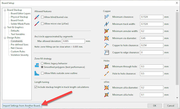
Here at River Loop, we’ve taken this a step further, creating templates of two layer, four layer, and six layer boards with trace geometries, clearances, and fabrication tooling stackups for our favorite board houses. It’s a breeze to incorporate these settings into a new design using PCBnew’s “Import Settings from Another Board” option, available in the Board Setup dialogue.
Avoid designing with BGAs when you start out
Ball grid arrays are an increasingly common form factor for high density, extremely small IC designs. BGAs allow the designer to pack a ton of integrated circuit into a very confined space. They are also much trickier to place accurately when reflowing a board setup by hand. It’s certainly possible to design with BGAs, and to hand reflow them - you can find plenty of videos online showing how to do so. It’s just a lot trickier to get working correctly on a first pass.
We’d recommend, as a starting point, to forego using BGAs, or their cousins, chip scale packages (CSPs or WLCSPs). You can certainly progress to this point after you get some experience under your belt. It’s just generally a good idea to know what you’re doing before you go down a black diamond run, so to speak.
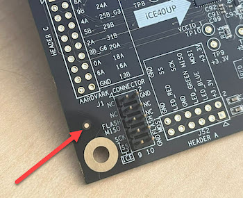
Include a fiducial
Fiducials are PCB features that help you align your board with external features, like stencils or PNP machines. They look like little bullseyes of copper circled with a void, or a soldermask etch. In effect, that’s what they are - if you can see your fiducial through your alignment feature, you know you have the proper datum between board and whatever external mechanical feature you must align to. We find that these are a huge help during the assembly phase, particularly when applying solder paste with a stencil. They also save you a step should you decide to ramp up production of your prototype at an external board house. You’ve already got alignment features baked into your design!
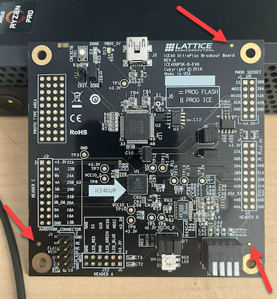
Be sure to include at least two fiducials; this makes it much easier to certify that you’ve achieved datum with the board surface.
Ordering Circuit Boards
Kit for a minimum of ten completed boards
You want to purchase enough components that you have plenty of component and board spares. This can help you validate whether you’re seeing an issue across multiple PCBs. It also never hurts to have a few backups on hand. I almost always make a careless mistake (sneezing, bumping a board, tripping over a door lintel) and lose the surface mount component I was holding at the time.
Spare bare boards are also a VERY handy thing to have around when the time comes to apply solder paste. More on that in the “Assembly” section.
Order a Framework Stencil
We frequently use PCBway for our prototype designs - the service they provide is very affordable, and very, very quick for simple two layer and four layer boards.
However, I maintain that the real hero of PCBway’s service isn’t their boards. It’s the stencils. For a mere $15, you can get a framework stencil included with your design.
In terms of incremental value, the $15 spent on a stencil is some of the best money you’ll spend over the course of your project. Absolutely order a framework stencil! It’s the difference between your assembly process taking an hour, or a day. Instead of soldering with a length of wire, or meticulously dabbing solder paste onto every terminal with a syringe, you can instead squeegee solder paste across the whole board, and simply place your components daintily atop the resulting paste pads. Pure magic!
Note, however, that you want a framework stencil. This means PCBway does the work to mount their metal stencil sheet in a convenient rigid frame, with epoxy for security. This makes a huge difference in the stencil’s usability. Unframed stencils are floppy, and difficult to attach to a PCB without deforming.
PCBway also offers the option to have multi board / multi sided stencils, where the top side paste mask is in one area of stencil, and the bottom side is in another. The choice to do this is at your discretion - see earlier comments regarding multi sided assembly!
Add Fiducial Features to your Stencil
Stenciling is one of the major reasons we recommend adding fiducials to your board design. They make aligning your stencil with your board a breeze. It’s very simple to add a fiducial feature using PCBway. Just select “lasered through” when specifying your stencils. This provides you an easy visual reference for board/stencil alignment.
Review Your Components for Recommended Paste Thicknesses
Stencil thickness determines how much solder paste is applied to your PCB during the assembly step. A thicker stencil naturally results in more paste being deposited on the board. Check your part datasheets for recommended stencil thicknesses; most chip vendors will give a recommendation for stencil thickness in their part datasheet, or in their component catalog. (If they don’t, you can always cross reference your part against another manufacturer’s assembly recommendation. Analog Devices and Texas Instruments both have extensive libraries of chip geometries and recommended footprints; these frequently specify stencil and paste thickness as a matter of course.)
When in doubt, go with a thinner stencil! A thicker stencil will leave more paste behind after squegeeing, and excess paste can cause issues (particularly bridging/shorts) in fine pitch components. It’s also harder to get clean separation between the printed circuit board and a thicker stencil’s worth of solder paste; the stencil will occasionally smear the extra paste onto neighboring pins. We’ve found that it’s generally easier to handle having too little paste on the board rather than too much. You can always touch up solder joints that seem a bit dry with a soldering iron later, if you need to.
Ordering Components
Order spare components
Bare circuit boards are only as useful as the parts that go on top of them. Make sure you kit enough to build out your ten bare PCBs! Even if you don’t assemble every board, the spares can be useful in case you break or misplace components. (Like we said earlier - accidents, and sneezes, happen.) Better still, order a few spares beyond what you need to build ten boards. This helps you to build a library of spare components that are commonly used in your lab facility. Even though you’re technically supposed to leave a component kit intact, we’ve all been guilty of swiping a spare 10k resistor from a kit in the lab. You’ll be grateful you did when you’re under the gun to get another design working!
If you’re price conscious, you can always cut this down to a kit of 5 whole circuit boards. It’s up to you, but we rarely regret ordering more components. Better to have them and not need them, rather than need them and not have them!
Order DNP or debug components as well as ones you know you need
It’s not uncommon to design boards with spare components that are excess to requirements in your design. Components like this are typically used for debugging or testing, but not included in a production design. As a result, they typically get marked with an attribute like “DNP” (short for “Do Not Populate”) or “No Pop” in KiCAD.
The purpose of our quick turn designs is to rapidly validate some sort of hardware security methodology. Given that, and the fact that not all of the techniques we try may work, it makes a lot of sense for us to add a variety of NoPop components to board designs. These can be there for debug purposes, or even speculative hardware use. Here’s just a few of the spare DNP style components I’ve added to boards before:
- Extra pullups/pulldown resistors
- Extra bypass or decoupling capacitors
- Extra shunt resistors or cut traces
- Spare FETs / BJTs with pullups / pulldowns (easily invert signals)
- Spare logic gates or inverters
In any case - these spare footprints are no good to you unless you order components to populate them with. The whole point of this exercise is to rapidly develop electronic prototypes. Sitting around waiting for a Digi-Key shipment defeats the point!
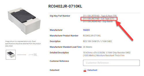
Choose “Cut Tape” for component packaging form factor
Digi-Key, Mouser, and other component vendors offer components in several packaging options. We almost always prefer “Cut Tape”, which specifies components arriving in small strips of plastic cellophaned into place. When we don’t use a pick and place machine, we’ve found reels are more trouble than they are worth.
Get board and reference designators printed on the bag
Digi-Key and Mouser will both print custom text on your component bags if specified properly. We always try to print the name of the circuit board, and the refDes’s of the components on the board, on the component bag. This helps keep track of the components with the box of kitted components, and can help you cross check where the components get assembled if you happen to start questioning your assembly process.
Kitting
Buy a container to store your parts + PCBs
Anyone who makes electronics has been guilty of repurposing Digi-Key boxes as their component kit storage system. And that’s OK! For a while, anyway. Eventually, you start accumulating so many kits that the mishmash of different-sized boxes becomes challenging to store and organize properly.
Spending a little bit of money on containers for your parts kits is money well spent in our experience. Sterilite makes great shoebox sized containers that fit the bill nicely for us - a set of a dozen will run you about $30-35, depending on where you buy them. (We use a 6-quart storage bin; they go for about $35 for a set of 12 on Amazon Prime.) Once you start accumulating a bunch of kits, a nice, regular sized box becomes a godsend - it’s easy to label, and easy to store in an inexpensive wire rack from your favorite local hardware store. Grabbing some standard rectangular labels and Sharpies are also a great move; this allows you to make nice, outward facing descriptive labels.
One other, important note: use one box per circuit board design. This helps us keep track of component inventories on a per-BOM basis. When possible, too, don’t combine orders from your component vendors. This makes reordering and stocking challenging. If you must combine, be sure to get your project name and reference designator info printed on the bag!
Add a BOM printout and a checkout sheet
Whenever we create a new storage box for a board kit, we add in a single top level sheet that’s summarized printout of the board’s BOM. This is easy to generate as a PDF or HTML printout from KiCAD. This should go inside your box of components, ideally right on top, or taped to the underside of the lid. This is a much faster reference than digging through the box to see what parts are inside - though you may have to do this anyway if your box contains the part you need.
It’s also helpful to add a checkout sheet. This is just a simple record of checkin/checkout that shows the number of kits that can be produced from the box, and who’s taken components from the box to build a board. You can templatize this in a Word doc, or just make one with markers and paper.
Add a board tracking sheet to each PCB’s ESD bag
Sometimes, when you’re working on a board that’s under active development, it’s helpful to go a step further in your tracking efforts. A tracking sheet can be a real boon in this scenario. A tracking sheet doesn’t have to be anything fancy; we usually just use a single piece of paper giving the status of the board. “Status” is generally pretty fungible. Useful things we’ve found to record on the tracking sheet:
- Functionality: working/not working?
- Test/bringup status: Tested/untested?
- What’s been done to it? Bodges? Rework steps? FW images flashed onto the board?
It’s a great idea to have this sheet accompany the board throughout its life cycle. If you’re ESD bagging your boards (and you should be!), it’s natural that the tracking sheet lives inside the ESD bag.
Assembling Your Boards
Equipment
Heating / Reflow
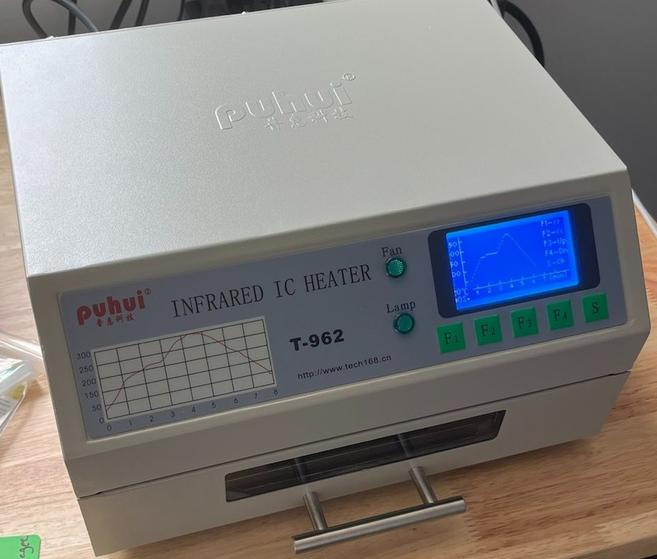
We have a few different tools of the trade when it comes to reflow. Our typical choice is a Puhui T-962 IR reflow oven:
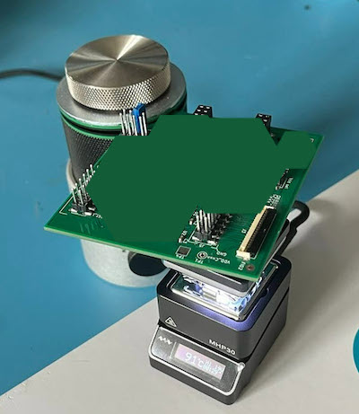
For smaller boards, or more local rework (i.e. heating up a board to lift a single component), we are huge fans of the MiniWare MHP-30 micro hot plate.
For larger reflow setups on a budget, a bigger hot plate can be a real advantage. Nathan Seidle of SparkFun wrote a lovely tutorial on repurposing a standard pancake griddle for reflow. Be sure to pick up some clean, dry sand to go into the griddle during your reflow. As one of the top commenters mentions, the sand helps distribute heat evenly throughout the circuit boards, which helps counteract some of the local variations in griddle temperatures.
For small boards with fairly large SMT components like QFPs, we occasionally turn to our Quick 861D hot air guns, but we’ve found that this is a hit or miss method of assembly. You often end up blowing unsecured passives off the board as you do reflowing them onto it!
Fume Extractor
Don’t skimp on this. Solder fumes and flux are gross, and not a great thing to be breathing in long term. Cheap fume extractors are as little as $40 online. Don’t shortchange your health and safety!
Solder Paste
We have two standbys for solder paste at RLS:
- Leaded - Kester EP256 - https://www.kester.com/DesktopModules/Bring2mind/DMX/API/Entries/Download?Command=Core_Download&EntryId=1523&language=en-US&PortalId=0&TabId=96
- Lead Free - Kester R276 - https://www.kester.com/DesktopModules/Bring2mind/DMX/API/Entries/Download?Command=Core_Download&EntryId=930&language=en-US&PortalId=0&TabId=96
Take note: if you’re making a design to hand off to a customer, be mindful of your RoHS requirements. A board that’s required to be lead free can’t be certified as such if it’s assembled using equipment that’s come into contact with leaded solder. Use caution!
Magnification
Placing 0402 components with the naked eye is possible, but I wouldn’t classify it as “fun”. A good visual magnifier makes the process a whole lot easier. Headband magnifiers are a good, affordable option. Some folks like using USB microscopes. I, personally, do not - they have just enough lag to be problematic with my hand/eye coordination. If you find yourself doing lots of rework and assembly, a proper stereo microscope is an invaluable tool. We have a few Amscopes laying around for just such a purpose!
Hand Tools
A good pair of tweezers is essential when placing SMT passives like resistors and capacitors. A vacuum pen is another handy thing to have nearby, for IC placements.
Procedure
Step One: Set Up Your Stencil
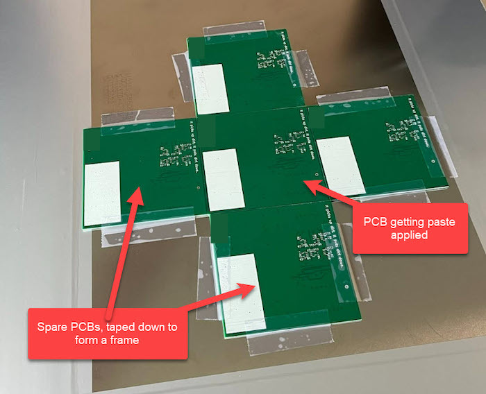
When you’re ready to start assembly, take a moment to tape some spare PCBs around the solder stencil area. This helps provide a level surface for the stencil to rest on, so that it doesn’t wobble and mess up your paste.
If your board is square or rectangular, you can take this a step further, and use a few of your spare PCBs to make a “frame” for the board under assembly. This helps keep the board under assembly aligned in the stencil cutouts, and it makes paste application for a small assembly run much faster. You don’t have to be nearly as careful aligning subsequent boards once the frame is made - you just pop the pasted board out, and pop the next one in!
PCBway sends excess scrap particle boards originally used for drill backing as packaging reinforcement for their stencils. We call this the “drill board”, and if you’re using the frame method we describe, we recommend saving it. When used in tandem with the PCB frames, it helps keep the board in place during paste application, or when the frame is being flipped. Image below shows the drill board backing the pasted board in the stencil.
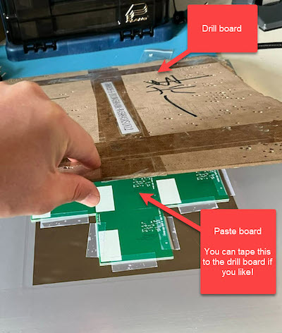
You can optionally tape the board that’s getting pasted to the drill board as well. This allows for a clean separation between pasted board and stencil when the stencil is lifted away. This can prevent globbing between close/adjacent footprint pads.
Step Two: Set Up PNP Sheets
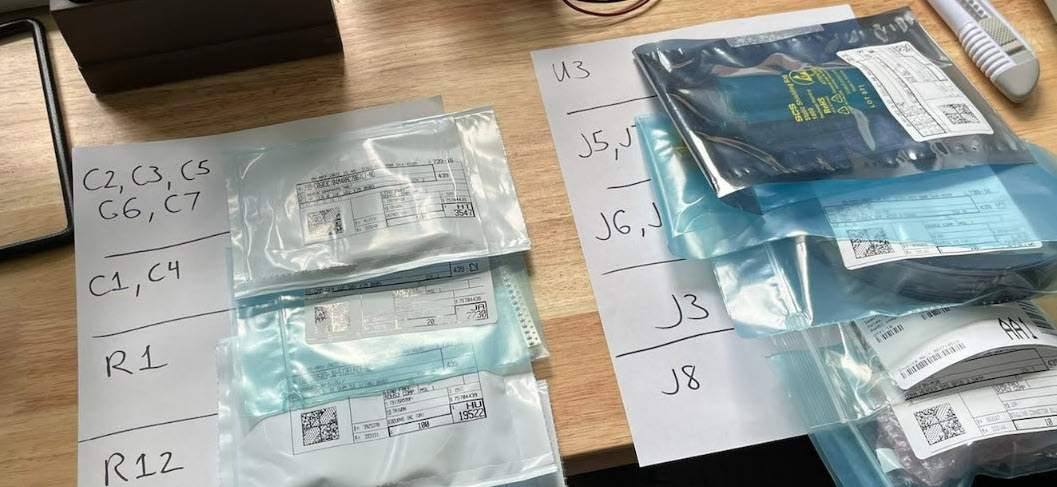
A big part of the time savings we garner through this process is saving ourselves the time and coordination required to set up a pick-and-place machine. As a result: we end up doing a lot of hand placements. We’ve learned through hard-won experience that component placement is one of the most difficult parts of this process - mostly because it’s so easy to become confused, and mix up different paper tapes of components.
To combat this, and reduce the odds of getting two component tapes mixed up, we’ve created a system that we refer to as “PNP sheets”. In addition to your kit of components, you’ll need a few sheets of letter sized paper, a marker, and some tape.
- Draw a few big lines across your sheet of paper, dividing it into four or five sections.
- Grab your first bag of components from your kit.
- Copy the list of reference designators that these components occupy onto the left side of your PNP sheet. (This is a snap if you’ve gotten the refDes printed on the component bag!)
- Tape the bag of components to the right side of where the refDes are written.
- Repeat with your bagged components, and sheets of paper, until you have a
prepared set of PNP sheets, like so:
Step Three: Apply Solder Paste
When you’ve got your frame locked and loaded, and your PNP sheets ready to go, it’s time to apply paste. Dispense a good sized blob of solder paste onto the top side of your stencil, and gently spread it across the stencil aperture. A “squeegee” of sorts is really useful for this. Chip-Quik and other solder vendors sell dedicated squeegees, but you can get equally good results from any flexible piece of plastic. I use an old transit system card, and it works great!
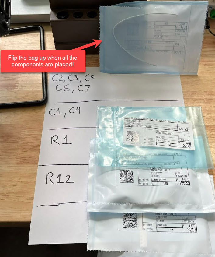
Step Four: Place Components
Once your board is pasted, you’re ready for placement. Grab your favorite tweezers, a vacuum pen, and a microscope - it’s time to put your PNP sheets to work! With a PNP sheet, you simply go down each sheet, line by line, grabbing one tape of components at a time. When you’ve placed all the components in a tape, you simply slide it back into its vendor bag, flip the bag up on the PNP sheet, and continue to the next bag/tape of components. This is what your kit sheet looks like after you’ve placed C2, C3, C5, C6, and C7.
If you really want to supercharge the placement process, consider using the InteractiveHtmlBom plugin for KiCAD. This handy tool makes it a snap to highlight component locations on a printed circuit board. If you’re clever, you can order and group your PNP sheets in such a way that you can go line by line through the PNP sheet and Interactive BOM in tandem with one another. It really makes hand placements a breeze!
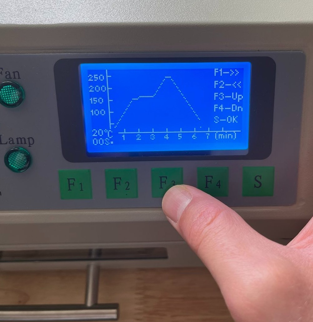
Step Five: Reflow
Once all of your components are placed, you’re ready to reflow. Move your board - carefully! - to your reflow equipment of choice. Dial in your temp profile, set your temperature, and give your board a minute. Some patience will be necessary; most solder pastes have a thermal profile that requires about 5-10 minutes from start to finish (check your solder paste’s datasheet for details on this!).
You also may need to do a bit of trial and error to get your thermal profile completely dialed in. When we started using our Puhui oven, we found that its default profiles were just a little too hot for leaded solder (it was burning plastic components during the peak of the profile), and a little too cool for lead-free solder (it wasn’t melting all the solder paste). Don’t be afraid to experiment, and modify to get good results!
Step Six: Cooldown, Inspection, and Test
After your heating process is complete, turn off your reflow element, and give it a minute. You’ll burn yourself if you get too excited! Jeez.
When the boards are cool enough to handle, have a good look at the solder joints under a microscope. Does everything look OK? Did all of your solder paste melt and reflow smoothly? Do you notice any bridged pins on a TFP or QFN package? What about incomplete joints? You can tidy these things up in a jiffy with a soldering iron.
You also want to check if anything major shorted together. Grab your multimeter and check your power rails. Are any of them shorted together that shouldn’t be? What about resistance to ground? Do all of your power rails have a nice open circuit resistance to your ground plane? It’s much easier to find out this way than firing up the board and letting out the magic smoke.
Once you’ve convinced yourself that everything is A-OK in your assembly process, it’s time to test your board!
More Info
The fine folks at Adafruit have likely forgotten more about SMT manufacturing than we here at River Loop will ever know. They also have a lovely, very detailed tutorial on SMT assembly. Check it out!
As a note, we’re currently hiring a hardware lab technician as well as vulnerability researchers and reverse engineers - reach out if you have interest!