By Sue Mohieldin | May 6, 2021
Introduction
Welcome back to our introduction to hardware hacking series! In this post we will be covering the Joint Test Action Group (JTAG) interface, its state machine, pinout, and electrical characteristics. This is the first part of a multi-part series about JTAG. In this first installment, we provide background and information to get started working with JTAG. In our next post, we will share a teardown of a TP-LINK AC1750 to demonstrate how to identify and verify a pinout for JTAG. Lastly, we will provide examples of how to use this for security research purposes to dump firmware, read and write memory, and perform other actions.
If you haven’t already, make sure to check out our other intro to hardware hacking posts on our blog.
JTAG Background
JTAG is a hardware interface that was developed by the Joint Test Access Group in the 1980s to address the technical challenges and limitations of testing interconnects on the increasingly complex, miniaturized printed circuit boards (PCBs). Methods such as bed-of-nails testing and external probing of PCBs became progressively time consuming, inefficient and even impossible with some integrated circuit (IC) packaging formats. One of JTAG’s most common uses, boundary scan testing, was designed to test interconnects on PCBs through a a single access port. Today, JTAG is used for programming, debugging and testing PCBs.
Boundary Scan Testing
Boundary scan testing was created as an easy way to test for electrical connectivity between components on complex PCBs. It works by clocking data through a long register connected to one or more components and comparing the input and output to assure that there are no faults. JTAG specifies a boundary scan architecture which consists of:
- A Shift Register: A large shift register connecting all components
- Cells: The components connected to the shift register
- A Test Access Port (TAP): The port for connecting to the shift register, in this case a JTAG port
The boundary scan test architecture incorporates boundary-scan (logic) cells placed between the IC’s core logic and the I/O pins or balls (the chip’s boundary). The cells are created using multiplexer and latch circuits and form a serial test data path throughout the IC. Under normal operation the cells act as pass through components for data on the shift register. The cells are capable of capturing or forcing data onto pins by serially shifting the data in or out of the boundary cells. The chip architecture is shown in figure 1.
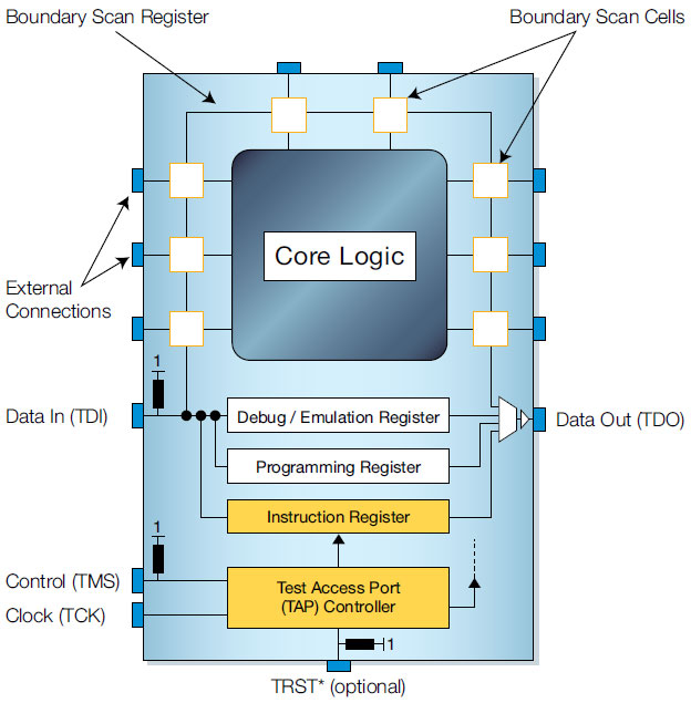
Figure 1: JTAG Chip Architecture. Source: XJTAG
In boundary scan testing between two JTAG devices, a diagnostic signal is sent to the test data input (TDI) pin. The boundary scan cell captures the signal and serially shifts it through the core logic. The output is then serially shifted through the core logic and out of the test data output (TDO) pin. This process is shown in figure 2. The output is then compared to the expected result. If the output matches the expected data then the boundary scan test passes, otherwise there is a fault such as a short, open or defect.
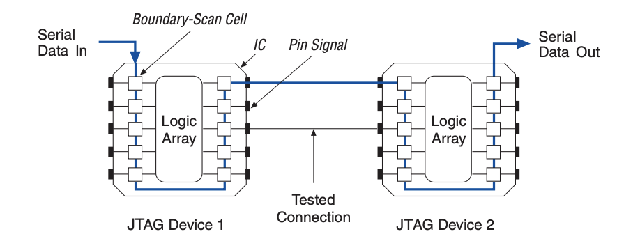
Figure 2: Boundary Scan Testing. Source: Intel
JTAG Signals
The primary JTAG Test Access Port (TAP) requires five signals each with its own hardware pin. These signals are detailed in the table below:
JTAG Pinout Table
| Pin | Description |
|---|---|
| Test clock (TCK) | Synchronizes the internal state machine of the boundary scan systemTerminated with 68 Ω resistor in series with a 100pF capacitor to GND |
| Test Mode Select (TMS) | The control signal for the TAP controllerSampled at the rising edge of TCK Has an internal pull up resistor, hence the signal is high with no input Usually has a 10k Ω pull up resistor on the line |
| Test Data Input (TDI) | Receives serial input data and shifts the data into the chipHas an internal pull up resistor, hence the signal is high with no input Data is sampled at the rising edge of test clock Usually has a 10k Ω pull up resistor on the line |
| Test Data Output (TDO) | Outputs serial data and can feed the TDI input of another JTAG device (if daisy chained)Data sent to the TDI pin will also appear at the TDO pin and is usually shifted by a number of clock cycles due to the length of the internal register Data is shifted out on the falling edge of TCK Tri-stated if data is not being shifted out of device Usually has a 10k Ω pull up resistor on the line and a 22 Ω series resistor near the next device in the JTAG chain, if applicable |
| Test Reset (TRST) | An optional signal that can be used to asynchronously reset JTAG test logic to a known state Usually has a pull down resistor |
State Machine
The TAP controller is a 16 state finite state machine (FSM) that is clocked on the rising edge of TCK and uses TMS to control the logic. As shown in figure 3, the state machine consists of two paths through two types of registers: a data register (DR) and an instruction register (IR). Data registers consist of boundary scan registers, bypass registers, and device ID registers (other types of registers also exist but these are the most common). Boundary scan registers allow for testing interconnects by moving data to and from the I/O pins. The bypass register supports a single bit scan path between TDI and TDO, reducing timing overhead when testing a circuit. The device ID register is 32-bits and stores information to identify the device such as device manufacturer, part number and version. This register supports “IDCODE” functionality. The instruction register has a minimum length of 2 bits, holds the current instruction/ operation and determines the action that will be performed and which data register will be accessed. Typically, an IR consists of a hold register which stores the previous instruction and a shift register, which shifts the next instruction.
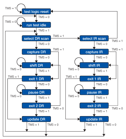
Figure 3: JTAG State Machine. Source: XJTAG
The following table explains the different states and pathways of the state machine:
State Machine Description Table
| State | Description |
|---|---|
| Test-Logic-Reset | Test logic is disabled, allowing for normal operation of the IC. At startup, TMS is driven high for at least 5 TCK cycles (or by holding TRST pin low) to ensure that the state machine is at this state and that the IC operates normally. |
| Run-Test // Idle | First state to begin test logic, default is idling state |
| Select-DR-Scan // Select-IR-Scan | Starting states for accessing data or instruction registers. Select-DR-Scan, controls whether to enter the data path or Select-IR-Scan state. If Select-IR-Scan is entered the controller can either enter the instruction path or return to the Test-Logic-Reset state. |
| Capture-DR // Capture-IR | In the Capture-DR state, test data is loaded in parallel into the data register. In the Capture-IR state, (fixed) data is loaded in parallel and ‘01’ is loaded as the last two significant bits for fault isolation |
| Shift-DR // Shift-IR | Data is shifted from TDI (on the rising edge of TCK) to TDO (on the falling edge of TCK). TMS is held low until shifting is complete |
| Exit1-DR // Exit1-IR | Temporary state where the state machine can either enter a pause state or an update state |
| Pause-DR // Pause-IR | Data shifting from TDI to TDO is temporarily halted |
| Exit2-DR // Exit2-IR | Temporary state where the state machine can either return to the shift state or an update state |
| Update-DR // Update-IR | In the Update-DR state, data is latched, preventing changes at the parallel output of the registers during the shifting states. In the Update-IR, data is latched and this data becomes the current instruction |
One thing to note is that JTAG allows for multiple targets (chips) to be daisy chained, and they can all be controlled through a single JTAG test access port (figure 4). The TDO of the first device is connected to the TDI of the second device, while TMS, TCK and TRST are parallel. The beauty in daisy-chaining multiple chips (all with JTAG capabilities) is that you can test all the different devices through a single connector on the board.
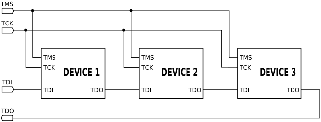
Figure 4: Daisy Chained JTAG. Source: Wikipedia
JTAG and Hardware Security
When it comes to hardware security, an unsecured JTAG interface can present significant cybersecurity risk. It may allow attackers to extract firmware, read and write memory, change the program counter, and ultimately have complete control over the device.
The first step to exploit an unlocked JTAG port is to identify the pinout and connect to it. In the following section, we will discuss how to identify a pinout for JTAG on an unknown target.
JTAG Connectors
The first step to accessing JTAG is to correctly locate the header and identify the pinout. In many cases, the JTAG pins are broken out on a single header and follow a pinout that consists of two rows (often 0.1 inch pitch or finer). Some common headers are 2x5, 2x7, 2x8 or 2x10 pin interfaces. Often, there are multiple GND pins on the header (for noise reduction), a Vcc/ Vref pin, as well as pullup resistors that range from 1-100k Ω near TMS, TDI and TRST (TDO is high impedance). A few examples of different interfaces are shown in figure 5.
It’s important to note that these are just a few examples and JTAG connectors can differ for different devices, designs, vendors and chip architectures. However, all JTAG interfaces will feature the 5 key signals: TCK, TMS, TDI, TDO and TRST (option).
One method to figure out the pinout is to trace the header to the chip on the PCB. By identifying the chip architecture, one can often map that to one of the ‘standard’ pinouts, (i.e. ARM, MIPS, or vendor-specific configurations). Another method is to measure the voltages and resistances of the pins, identify GND, VCC, and the pull-up or pull-down resistors in use, and then compare that to known JTAG port configurations.
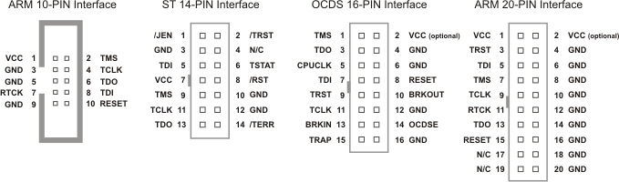
Figure 5: JTAG Interfaces. Source: armKEIL
The next step once a potential pinout is identified is to attempt to establish a connection with a JTAG debugger. We’ll cover that in Part 2 of our series. In the meantime, feel free to contact us with any questions about how we can help access or secure many types of access to embedded devices and other connected systems.