By Anthony DeLorenzo | February 11, 2020
Introduction
Welcome back to our series on an introduction to hardware hacking! In this post we will be covering the Serial Peripheral Interface (SPI) protocol, a commonly used serial bus protocol which allows hardware components to communicate with each other.
The goal of this post is to serve as a guide for security researchers and hardware hackers to easily interface with target devices. Many embedded devices use SPI to access persistent data stored on flash memory. As a result, being able to interface with devices using this protocol allows reading and writing of firmware, which can be crucial to further security analysis.
SPI Background
The SPI protocol is a 4-wire and full duplex (receive and transmit simultaneously) bus protocol developed by Motorola in the mid 1980’s. It has since become a widely used protocol for short range high speed serial data transmission due to its high data throughput and reliability. Since we are examining SPI from an attacker’s perspective, we can ignore many of the design considerations taken into account when designing a PCB, such as space and power consumption. A non-exhaustive list of devices commonly built on SPI include some kinds of non-volatile memory (ROM, EEPROM, Flash), LCD displays, and various sensors. The most interesting for our purposes is non-volatile memory, as this is commonly where device firmware is stored in a persistent manner waiting to be analyzed for vulnerabilities.
Prior to diving in, we will go over a few prerequisites such as SPI signal lines, command timing from device datasheets, and logic analyzer traces. This will arm you with the skills needed to recognize SPI if you encounter it, even when datasheets are nowhere to be found and you’re working with an unfamiliar PCB.
SPI Signal Lines
SPI flash interfaces commonly function by a “master” device writing commands (such as read, write, or erase) to a “slave” device. The slave device listens for these commands and relays the response data to the master device. This communication operates over four very recognizable main signal lines along with a few other peripheral lines. Their functions are described below. Since there is no officially defined and adopted standard for SPI, the exact names and abbreviations often vary by manufacturer. We’ve included the most common ones but you may encounter a signal line not listed. Simply match the described or observed functionality with the ones listed below:
SPI Pin Description Table
| Names | Function |
|---|---|
| CS (Chip Select) SS (Slave Select) CE (Chip Enable) | Selector for which slave device the master wishes to communicate with. Each slave has their own CS input. Slave will only listen to commands if it’s corresponding CS is selected. |
| SCLK (SPI Clock) | Clock line used to synchronize data transmission between master and slave device. |
| MOSI (Master Out Slave In) DI (Data In) SI / SDI (Slave In / Slave Data In) MO (Master Out) | Data transmission line using the slave as a sink and the master as a source. |
| MISO (Master In Slave Out) DO (Data Out) SO / SDO (Slave Out / Slave Data Out) MI (Master In) | Data transmission line using the master as a sink and the slave as a source. |
| HOLD | A switch to stop all serial communication. For our purposes this will either be statically pulled high or low. Different chips use either logic high or low for this value, so the best way to tell is to examine logic traces or chip datasheet. |
| Write Protect (WP) | Stops writes to SPI flash data. Sometimes you can leave this pin floating (not connected to anything). Best practice is to pull in the direction observed in logic analyzer. |
Timing
The first pin to change state in a SPI transaction is always the CS (Chip Select) line. Other devices will vary but when dealing with SPI flash, the most common flow you will encounter is as follows:
- Desired slave’s CS line is selected (pulled low usually).
- Master starts driving the SCLK line.
- Master sends command on the MOSI data line.
- Slave sends command response data on the MISO line.
- Master either sends another command or deselects the selected CS line.
Datasheet Timing Example
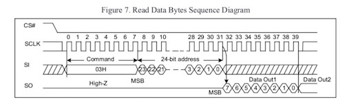
SPI timing diagram from GD25Q32 Datasheet
When a logic analyzer trace shows some sort of data transmission, looking for these timing and pin markers is useful in determining whether or not the protocol you’re seeing is SPI.
Hands On
Let’s take a look at the same TP-Link N300 router as our first hardware hacking series post. We will focus on dumping firmware by interfacing with the onboard SPI flash chip.
Materials
The following materials are needed to follow along with this tutorial. You can pick these or other products that serve the same purpose. Links are included just for your convenience:
Needed to Follow Along
Reccomended for Starter Hardware Lab
In addition to the above, we will need some way to interface with the SPI flash chip. Some tools that are suitable are listed below and will be covered in this post:
Raspberry Pi
The Raspberry Pi has long been a widely used single board compute platform for both software and hardware projects. The newer models contain many features far beyond the scope of this post. The Raspberry Pi’s GPIO pinout can be viewed at https://pinout.xyz/.
GoodFET
The GoodFET is a tiny adapter board that facilitates access to various hardware bus protocols such as JTAG, SPI, and I2C. It is not a full single board computer like the Raspberry Pi and thus does not cover as wide a range of use cases. However, it does provide a smaller footprint and more efficient way to interface with hardware targets and is a good tool to use if your needs are constrained to interfacing with PCB components.
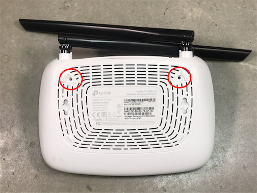
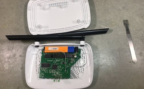
TP-Link WR841N: Disassembly
First step to any device hardware hacking session involves tearing down the outer casing to gain access to the internal PCB. In this case, start by removing the two screws on the bottom of the device as shown below:
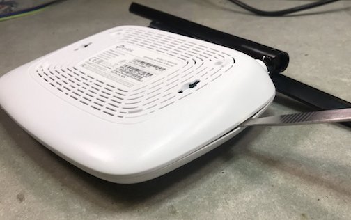
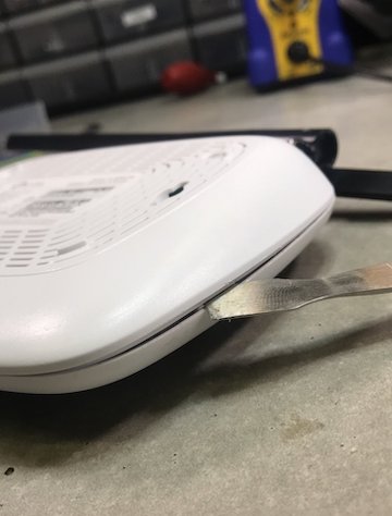
Next, insert a rigid tool along the routers edge to begin popping out the plastic clips holding the two-piece case together. After the tool is inserted, slide along the edge to pop out the first clip. The first clip is the most difficult one, the ones after that will become much easier.
After popping all of the clips off, the two-piece case will separate and reveal the internal PCB:
TP-Link WR841N: PCB Examination
After disassembly, let’s start examining the PCB to see what components make up the TP-Link N300 device. The image below is labeled with each component type:
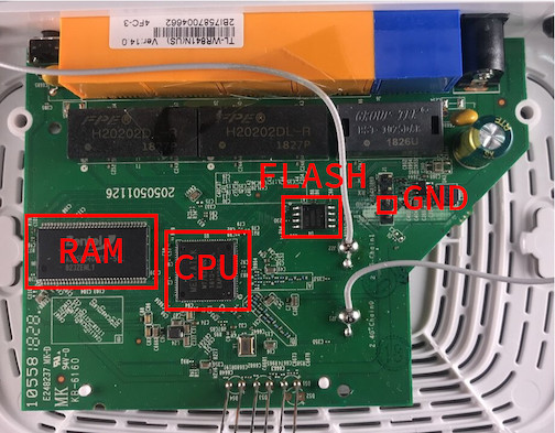
For this post, we’re most interested in the flash memory. This is where all the device code and persistent data are stored.
The part number for that chip can be read in this image (Giga Device 25Q32CSIG):
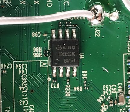
I urge you to search around to try and find an exact or chip family data sheet. We will be continuing as if we do not have a datasheet since many times when you’re attacking devices you will not have access to a chip datasheet.
TP-Link WR841N: Logic Analyzer Setup and Walkthrough
One thing that will make your life infinitely easier is using one of these 8 pin clips (listed in materials!) to clip on to the SPI chip. It’s much easier and faster than soldering wires to the chip, and often will let you dump firmware without requiring any soldering at all.
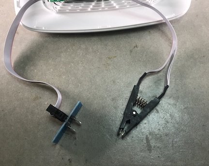
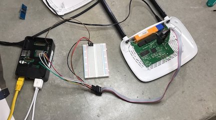
Our next step is to wire the logic analyzer to the SPI device. We used the pin headers soldered in our previous Hardware 101 blog entry for a logic analyzer ground reference. The remaining wires are run to the clip which is attached to the target flash chip.
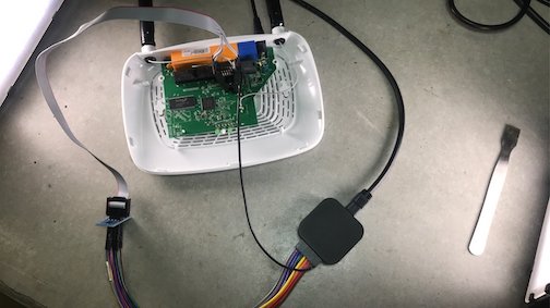
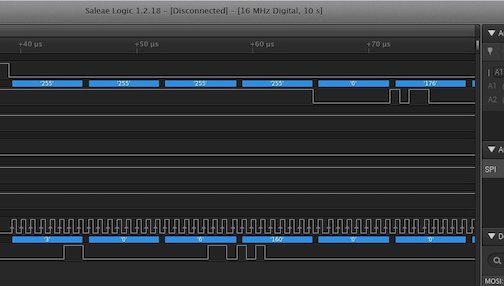
Start a capture and turn on the device. You should see something similar to the traces below:
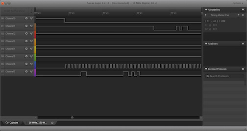
TP-Link WR841N: Trace Breakdown
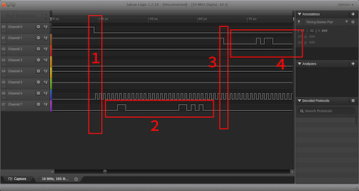
We can see a textbook SPI transaction take place which will tell us the corresponding pins to connect to our flash reader.
To walk through these in more detail:
- First, the CS (Chip Select) pin is pulled low and the SCLK (SPI Clock) starts oscillating. This gives us valuable information that channel 0 is the CS pin and channel 6 is SCLK.
- Next, the master begins sending a command to the flash chip. Channel 7 is MOSI.
- The master’s command is done (4 bytes long, 32 bits) marking the beginning of the slave’s response. Channel 1 is MISO.
- Slave continues sending the response.
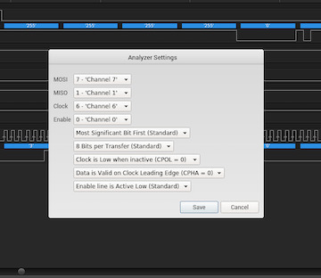
Using this valuable information we can add an analyzer to our logic trace. This will let us confirm whether or not our pin assignments are correct. To do this, click the plus shown on the right hand side of the logic analyzer client as shown below then click on SPI:
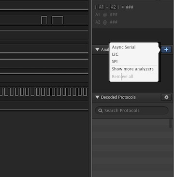
Next, fill in the details that we’ve recovered using the logic trace denoting which channels correspond to which pin. The defaults for anything we don’t know should suffice. After finishing and clicking “Save”, we should see successfully decoded SPI data shown informing us that our pin assignments are correct.
Channels 2, 4, and 5 are all pulled high. These correspond to HOLD, WP, and VCC (Power). We will wire all of these high when we read the flash to match its normal operating conditions. The last channel, channel 3, is pulled low – this must be ground. The following table shows which channels are matched to which pins judging solely on this one logic analyzer trace. The listed Raspberry Pi pins should be confirmed using https://pinout.xyz since they might change with new revisions.
Trace Mappings
| Channel # | Assignment | Raspberry Pi Pin |
|---|---|---|
| Chan 0 | CS | Pin 24 |
| Chan 1 | MISO | Pin 21 |
| Chan 2 | WP or HOLD or VCC (Wire high) | Pin 1 |
| Chan 3 | Ground (Wire low) | Pin 39 |
| Chan 4 | WP or HOLD or VCC (Wire high) | Pin 1 |
| Chan 5 | WP or HOLD or VCC (Wire high) | Pin 1 |
| Chan 6 | SCLK | Pin 23 |
| Chan 7 | MOSI | Pin 19 |
Before we start dumping the flash data, be careful that you do not confuse channel numbers with pin numbers. Channel 7 on the logic trace does not always mean pin 7 on the target chip (unless you have it wired that way). It is extremely helpful and recommended to get a piece of paper and draw out your individual wiring setup.
TP-Link WR841N: Dumping SPI via Raspberry Pi
You will need to enable SPI on the Raspberry Pi if you haven’t done so already. This can be done by running ‘sudo raspi-config’. Select ‘Interfacing Options’ and then select ‘SPI’.
Now that we know which pins are assigned to which channels, we can wire up the target device to a Raspberry Pi and read the flash contents. The Raspberry Pi GPIO (General Purpose Input Output) pinout can be viewed at https://pinout.xyz/. Click on “SPI” on the top navigation to see which GPIO pins are used for SPI. Make sure that you connect each wire to the corresponding SPI interface.
For example, if you connect MOSI to GPIO pin 38, which is SPI 1 MOSI, all the other pins also need to be connected to the SPI 1 pins: SPI 1 MISO, SPI 1 CS, and so on.
Reading SPI FLash Using Flashrom
After setting up the wiring, we are ready to read the target flash device. To do this, we use flashrom, a program which reads various flash chips with a very large repository of supported devices. You can read more about flashrom here: https://www.flashrom.org/Flashrom. It can be installed on Linux with sudo apt install flashrom.
Once you’ve installed flashrom and set up the Raspberry Pi SPI interface, run the following commands:
# NOTE: Make sure the spidev you give to flashrom matches your wiring.
# IE: If you wired CS to ‘SPI 1, CE 0’, then give flashrom
# /dev/spidev1.0. For SPI 0, CE 0, give flashrom /dev/spidev0.0

user@raspberrypi:~/spi $ sudo flashrom -r TP_LINK.img -p linux_spi:dev=/dev/spidev0.0,spispeed=8000
[sudo] password for user:

flashrom  on Linux 4.19.75-v7+ (armv7l)
flashrom is free software, get the source code at https://flashrom.org

Using clock_gettime for delay loops (clk_id: 1, resolution: 1ns).
Found GigaDevice flash chip "GD25Q32(B)" (4096 kB, SPI) on linux_spi.
Reading flash... done.
Note: If you are getting errors about not finding your connected chip, try the following:
- Double check wiring, especially ground.
- Check wire length, If wire length is super long you could encounter signal integrity issues.
- Make sure to include the spispeed=8000 argument for flashrom. Sometimes the Raspberry Pi will drive the SPI clock at too high of a frequency. This will cause the device to not respond properly to commands.
Once you’ve successfully read the flash, we can unpack it using binwalk. Binwalk is a very comprehensive file carver. You should be familliar with it if you’re constantly dealing with raw packed firmware.
# The -e flag is for 'extract' and the -M argument is for recursive. This will recursively extract all things that binwalk finds. (IE: If it finds a filesystem in the image, it will also unpack the filesystem for you)
user@raspberrypi:~/spi $ binwalk -eM TP_LINK.img

Scan Time:     2020-02-07 17:58:50
Target File:   /home/user/spi/TP_LINK.img
MD5 Checksum:  4f3f9155313793a67c1857cd92c49606
Signatures:    386

DECIMAL       HEXADECIMAL     DESCRIPTION
--------------------------------------------------------------------------------
53440         0xD0C0          U-Boot version string, "U-Boot 1.1.3 (Mar 19 2018 - 09:23:08)"
66048         0x10200         LZMA compressed data, properties: 0x5D, dictionary size: 8388608 bytes, uncompressed size: 2986732 bytes
...
As this binary was straightforward to unpack, we now have access to the full device firmware!
user@raspberrypi:~/spi $ tree -d _TP_LINK.img.extracted/
_TP_LINK.img.extracted/
├── _10200.extracted
│   ├── cpio-root
│   │   ├── dev
│   │   └── root
│   ├── dev
│   └── root
└── squashfs-root
    ├── bin
    ├── dev
    │   ├── net
    │   ├── pts
    │   └── shm
    ├── etc
    │   ├── init.d
    │   ├── ppp
    │   └── samba
    ├── lib
    │   └── modules
    │       └── kmdir
    │           └── kernel
    │               ├── drivers
    │               │   └── net
    │               │       ├── raeth
    │               │       ├── rt_rdm
    │               │       └── wireless
    │               │           └── mt_wifi_ap
    │               └── net
    │                   ├── ipv4
    │                   │   └── netfilter
    │                   ├── l2tp
    │                   ├── netfilter
    │                   └── shortcut-fe
    ├── mnt
    ├── proc
    ├── sbin
    ├── sys
    ├── usr
    │   ├── bin
    │   └── sbin
    ├── var
    └── web
        ├── css
        ├── frame
        ├── help
        ├── img
        │   └── login
        ├── js
        ├── main
        └── xml

49 directories
user@raspberrypi:~/spi $
Reading SPI Flash Using GoodFET
NOTE: This is an alternate option to reading using Raspberry Pi. You do not need to do both.
The process of dumping SPI flash using the GoodFET42 is very similar to the Raspberry Pi. First, you must wire the target device to the GoodFET42. The pinout for SPI can be seen here: http://goodfet.sourceforge.net/apps/spi/.
You will need to flash (if your GoodFET isn’t already flashed with it) the GoodFET42 client software. Directions to do this can be found at: https://github.com/travisgoodspeed/goodfet.
Once you have everything functioning with your GoodFET42, the following commands can be run to dump the connected SPI chip:
[lab client]# export BOARD=goodfet42
[lab client]# python2 ./goodfet.spiflash info
See the GoodFET FAQ about missing info flash.
Ident as None None
Manufacturer: c8 None
Type: 40
Capacity: 16 (4194304 bytes)

[lab client]# python2 ./goodfet.spiflash dump ~/TP_LINK.img
Dumping code from 000000 to 400000 as /root/TP_LINK.img.
Dumped 000000.
Dumped 001000.
...

Dumped 3ff000.
After the command completes (takes longer than the Raspberry Pi), we can unpack the image using the same as above via binwalk:
[lab ~]# binwalk -eM TP_LINK.img

Scan Time:     2020-02-07 13:27:45
Target File:   /root/TP_LINK.img
MD5 Checksum:  4f3f9155313793a67c1857cd92c49606
Signatures:    391

DECIMAL       HEXADECIMAL     DESCRIPTION
--------------------------------------------------------------------------------
53440         0xD0C0          U-Boot version string, "U-Boot 1.1.3 (Mar 19 2018 - 09:23:08)"
66048         0x10200         LZMA compressed data, properties: 0x5D, dictionary size: 8388608 bytes, uncompressed size: 2986732 bytes
...

[lab ~]# tree -d _TP_LINK.img.extracted/
_TP_LINK.img.extracted/
├── _10200.extracted
│   ├── cpio-root
│   │   ├── dev
│   │   └── root
│   ├── dev
│   └── root
└── squashfs-root
    ├── bin
    ├── dev
    │   ├── net
    │   ├── pts
    │   └── shm
    ├── etc

    ...

    ├── var
    └── web
        ├── css
        ├── frame
        ├── help
        ├── img
        │   └── login
        ├── js
        ├── main
        └── xml

49 directories
Hack on!
In this post we’ve covered the process of locating the chip housing device firmware, using a logic analyzer to determine the functional mappings of it’s signal traces, and reading the housed firmware using two different tools. We then unpacked the firmware using binwalk allowing us access to the raw device filesystem.
From this point, all the code responsible for running the device is accessible for analysis. The next steps moving forward would include further analysis of device executables to search for vulnerabilities!
Be sure to check up on our next Hardware Hacking 101 post where we will be covering eMMC, another form of persistent device storage, which will add more techniques to your toolkit you can use to examine more complex and interesting devices.
We encourage you to contact us if you have any questions or comments based on this post or have questions about hardware reverse engineering or penetration testing.