By Cristian Vences | October 14, 2020
Introduction
Welcome back to our hardware hacking series! We are excited to share the “glitching” techniques we use in our device assessment process. Glitching, or voltage or fault injection, is the process of changing voltage levels in a digital system in a manner that causes disruption of the system under test or corruption of data. If timed correctly, a glitch of even 1 millisecond can cause a system to fail open into a potentially privileged state.
In this blog post we cover glitching on a D-Link router to achieve escalated privileges on the system. Topics will include digital logic analysis, flash memory, and bootloaders.
The Boot Process
Before we can get into glitching devices to give us privileged access, we must understand where and when digital systems are more vulnerable to unexpected voltage changes. Through some extensive research and a lot of hands on experience, we have found that when a device is booting up and initializing, it is in a vulnerable state. This is due to the fact that during boot, the CPU must request data from other chips on the device, such as flash memory, to access the bootloader and other parts of firmware that allow the device to complete the boot process.
Usually these CPUs have fail-safes whereby if they do not correctly communicate with the other chips on board, they default into a failed state. In this blogpost we will be targeting the communication between the flash memory chip and the CPU on the D-Link router and exploit the fail-safe mechanism when that communication is severed.
Hands On
Follow Along
Materials
- D-Link DAP-1650 Router
- UART-USB Converter
- Logic Analyzer
The Target
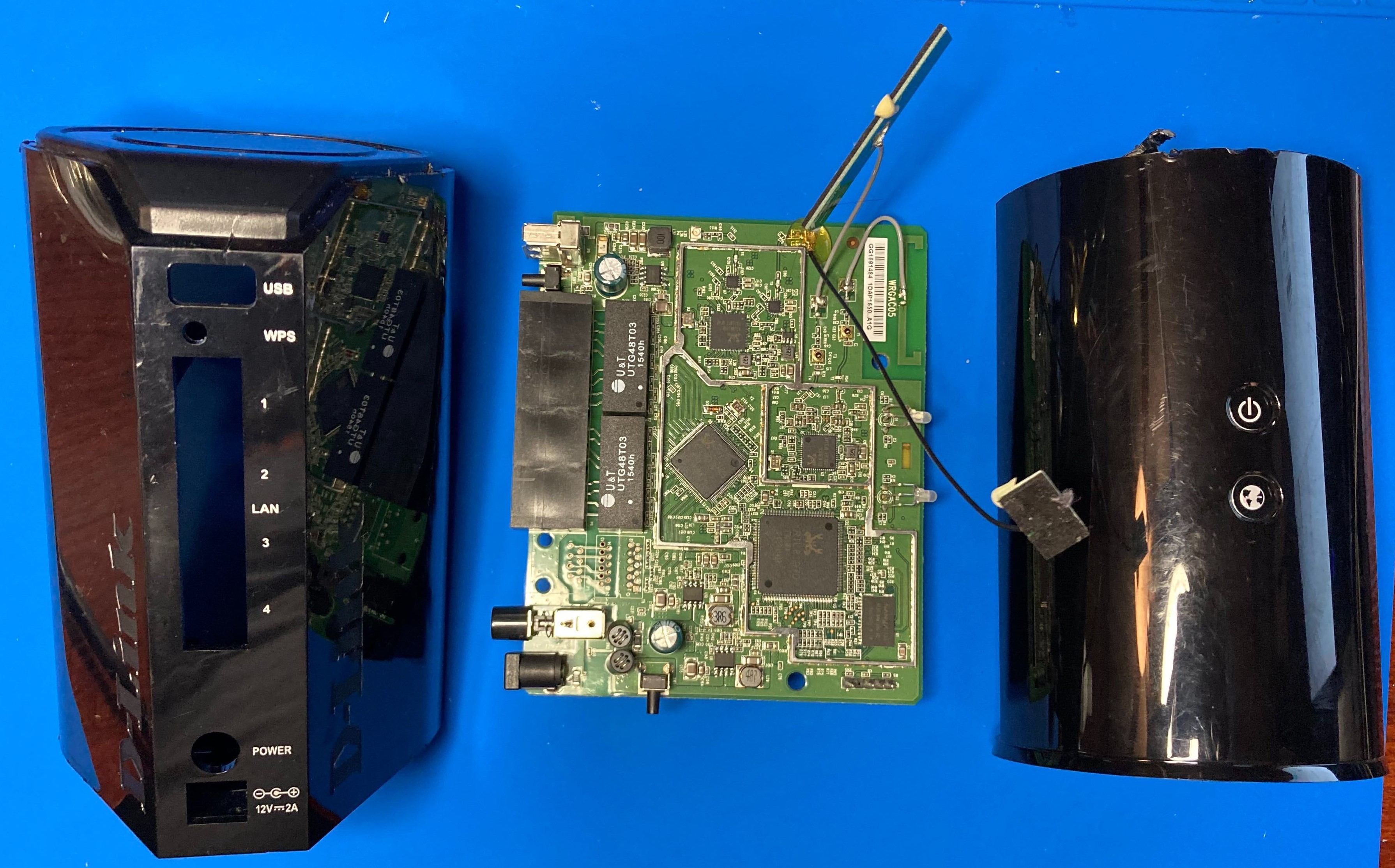
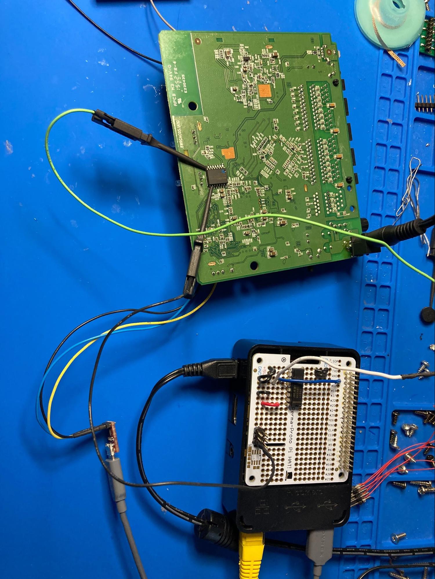
Today we will be attempting to get escalated privileges using electrical glitching techniques on a D-Link DAP-1650 router. After removing the screws from the top and bottom of the device and removing the PCB from the plastic enclosure, we are left with this.
The device has a RealTek CPU with a handful of other chips. We are going to focus on the SPI flash chip which is a Macronix MX25L that runs on 3.3v Vcc and has 128M-bit capacity. This router also has serial headers that we will use later to our advantage to get insights into the boot process and get privileged access to the system.
Reconnaissance
Using a serial UART to USB converter, we are able to receive the outgoing serial communication from the headers at JP1. In this post we do a brief tutorial on how to interface using UART – but a more in-depth tutorial can be found here.
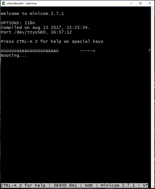
Connecting the serial UART to USB converter to a computer running Linux, we were able to view the boot logs disclosed on this header using a terminal emulator (in this case we use Minicom). Open up a terminal and here is the line of code to get that running:
sudo minicom -D /dev/ttyUSB0 -w -C D-link_startup.txt
We previously used a logic analyzer to find the baud rate which we can set in the minicom settings to 38400. Now we are able to receive the output from the transmit pin (TX) on the UART port. Let see what that gets us…
Booting...

@@@@@@@@@@@@@@@@@@@@@@@@@@@@@@@@@@@@@@@@@@@@@@@@@@@@@@@@@@@@@@@@@@@@@@@@@@@@@@@@
@
@ chip__no chip__id mfr___id dev___id cap___id size_sft dev_size chipSize
@ 0000000h 0c22018h 00000c2h 0000020h 0000018h 0000000h 0000018h 1000000h
@ blk_size blk__cnt sec_size sec__cnt pageSize page_cnt chip_clk chipName
@ 0010000h 0000100h 0001000h 0001000h 0000100h 0000010h 000002dh MX25L12805D
@
@@@@@@@@@@@@@@@@@@@@@@@@@@@@@@@@@@@@@@@@@@@@@@@@@@@@@@@@@@@@@@@@@@@@@@@@@@@@@@@@

---RealTek(RTL8196D)at 2013.07.05-14:42+0800 v0.5 [16bit]
(659MHz)
SVN:884 signature=wapac04_dlob_dap1650
Verifying Checksum ...

Checksum PASS.
CHECK FLASH IMAGE: SEAMA header was found!!
Read Addr =0x80500000! srcAddr=0x00050050 len =0x0016d000

Jump to image start=0x80500000...
decompressing kernel:
Uncompressing Linux... done, booting the kernel.
done decompressing kernel.
Alight! As usual, the serial port gives us some boot logs letting us know when and how the device is getting initialized. If you look closely, the boot logs indicate a checksum being calculated and validated. This usually occurs when the CPU is reading from flash and verifying the image. The checksum is computed to assure that what is read from flash is valid and intact.
This might be a great time to take advantage of a fail-safe mechanism and interrupt communication between the CPU and flash chip. We use a logic analyzer to view SPI communication between the flash chip and CPU as well as the serial output to get a better picture of what is going on electrically during boot.
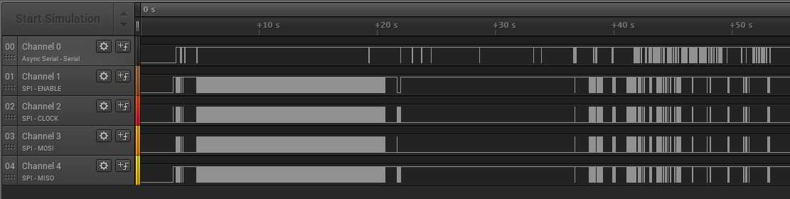
In our setup channel 0 is connected to the TX pin on the device and channels 1-4 are connected to the serial communication pins on the flash memory chip.
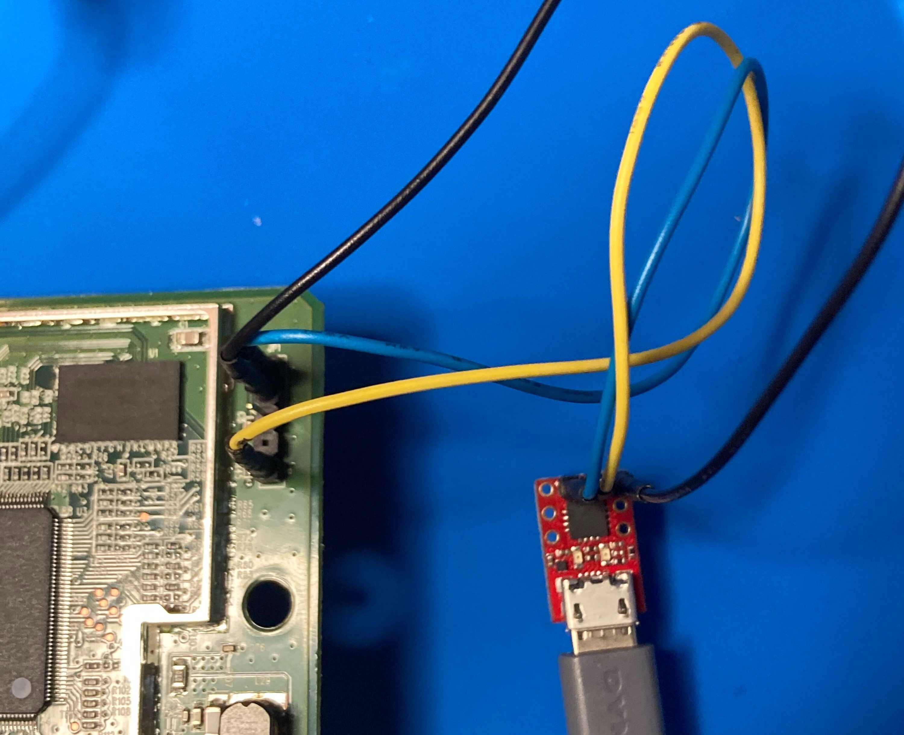
As you can see here, the flash memory has exposed pins which make it easy to clip on to with test clips.
Taking a look at this logic capture we can see lots of activity from the flash device roughly 2 seconds after boot. This is likely when the device is reading all the configuration settings that the CPU requires to boot the device properly. This is a great time to perform a glitching attack.
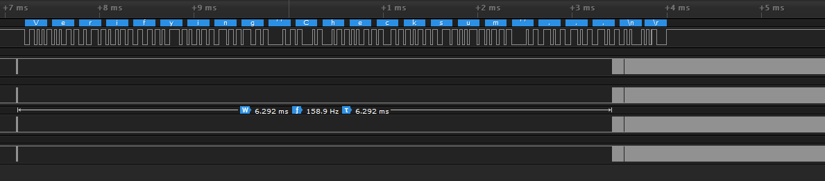
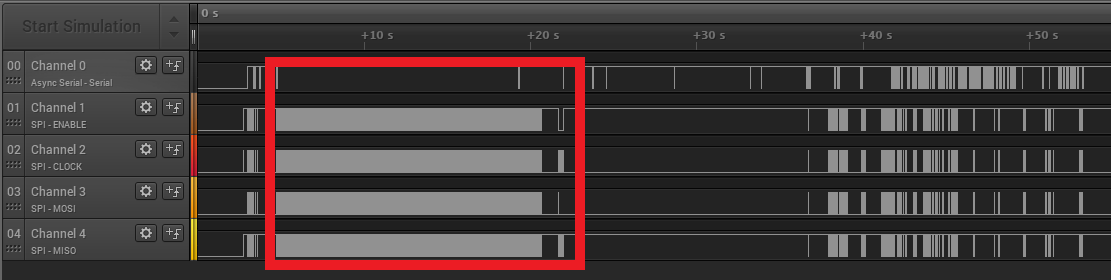
Zooming in we can see that this corresponds with the time that the serial logs say that the device is calculating a checksum. Let’s see what happens when we perform a glitching attack at this time.
Glitching
We perform glitching to change voltage levels in a digital system in an unexpected manner. There are many ways to glitch the device – but the easiest is to bridge the connection between a data pin and ground. This causes the data transmission to fail, allowing us to potentially exploit a device’s open failure into a more privileged state.
Here’s the setup:
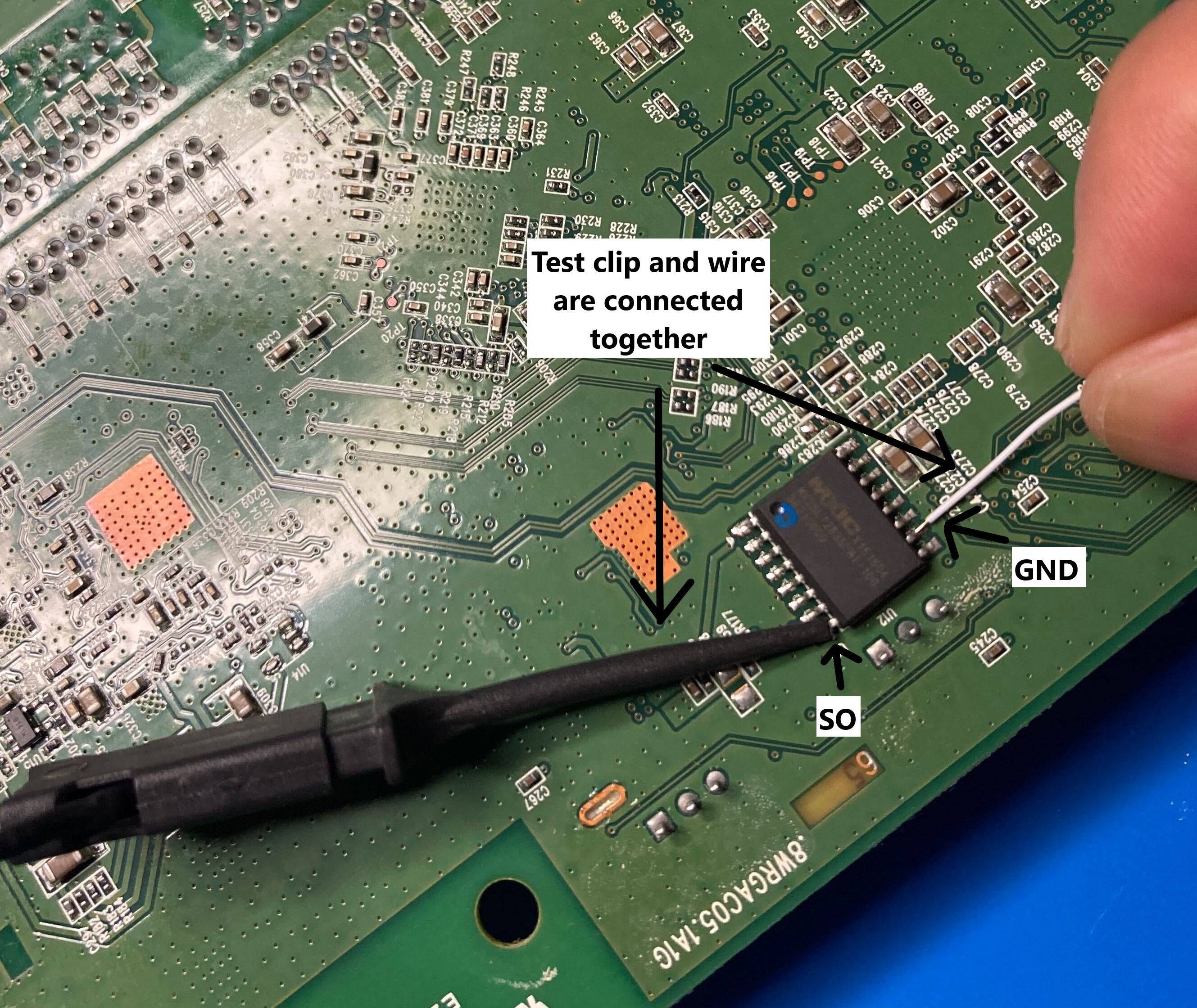
We connected a test clip to the SPI flash’s serial output (SO) pin and have an exposed wire connected to the clip. The exposed wire is used to touch and bridge the SO pin to the ground pin on the other side of the chip. When we do this, the serial output from the flash memory chip is disrupted, preventing proper communication between flash and processor. This must be a timed effort as we will bridge the connection right after the serial logs tell us that the device is calculating the checksum. By lining up with this calculation and corresponding serial output, we can be sure we’re disrupting a read of this flash chip during a critical boot operation.
Let’s give a try and see what is displayed in the serial console.
Score! Instead of proceeding with the boot process normally or failing because the flash was not read correctly, we are presented with the bootloader shell for the RealTek CPU. This gives us much more access to the system than we had before, all due to our well-timed glitching attack!
Let’s see what commands we have available.
<RealTek>?
----------------- COMMAND MODE HELP ------------------
HELP (?)                                    : Print this
help message
DB <Address> <Len>
DW <Address> <Len>
EB <Address> <Value1> <Value2>...
EW <Address> <Value1> <Value2>...
CMP: CMP <dst><src><length>
IPCONFIG:<TargetAddress>
AUTOBURN: 0/1
LOADADDR: <Load Address>
J: Jump to <TargetAddress>
SIG: SIG <type><sig>
SIGR: Display signature and flag
FLR: FLR <dst><src><length>
FLW <dst_ROM_offset><src_RAM_addr><length_Byte> <SPI cnt#
>: Write offset-data to SPI from RAM
MDIOR:  MDIOR <phyid> <reg>
MDIOW:  MDIOW <phyid> <reg> <data>
PHYR: PHYR <PHYID><reg>
PHYW: PHYW <PHYID><reg><data>
PORT1: port 1 patch for FT2
D8 <Address>
E8 <Address> <Value>
Now we have lots of new commands that we can use to make modifications or use restricted features of the device! Often, we find that access to a bootloader console allows us to modify boot parameters and obtain persistent root or other access on devices.
We hope that this tutorial showed you the process of successfully using glitching as an attack to gain privileged access to a system. However, we realize that successfully executing these attacks can be challenging, especially related to getting the timing of the attack right, which is why we’re introducing a new open source tool to help solve this problem!
Automate Glitching?
Introducing Flash BASH

We are excited to announce that we will shortly be releasing an open source tool that helps automate the process of glitching flash chips to get you into a bootloader shell.
The tool takes in serial input and automatically performs the glitching for you at exactly the right time based on corresponding boot logs from serial output. This is a Raspberry Pi based tool and requires a multiplexer that does the grounding for you as long as you have ground and data pin connected.
This tool is still in development. We have a few tweaks to before it is released but keep an eye on our blog and Twitter and you will be notified as soon as possible!