By Kareem ElFaramawi | March 9, 2020
Introduction
Welcome back to our introduction to hardware hacking series! In this post we will be covering embedded MultiMediaCard (eMMC) flash chips and the standard protocol they use. eMMC is a form of managed flash storage typically used in phones, tablets, and many IoT devices because of its low power consumption and high performance. If you haven’t already, make sure to check out our other intro to hardware hacking posts on our blog.
We’ll also be tearing down an Amazon Echo to show how to use logic traces to identify a pinout for an eMMC chip. Lastly, we’ll walk through options for dumping the contents of the chip while it’s still on the board, as well as when it’s lifted off.
MMC & eMMC Background
MultiMediaCard (MMC) is a form of solid-state storage originally created for use with portable devices, such as cameras. It features a low pin count, along with a simple parallel interface for communicating with it. This standard was later improved upon as the Secure Digital (SD) standard, which had much better performance while keeping the same simple interface. Often you’ll see that SD cards contain two primary components: a NAND flash chip, and a flash controller. NAND flash is a type of flash memory used in many embedded devices, typically seen in TSOP-48 or BGA-63 packages. Other types of flash memory include NOR flash and Vertical NAND flash. The NAND flash is the non-volatile storage where all of the data on the SD card is stored, while the flash controller provides an interface to the NAND flash in the form of the data pins on the SD card.
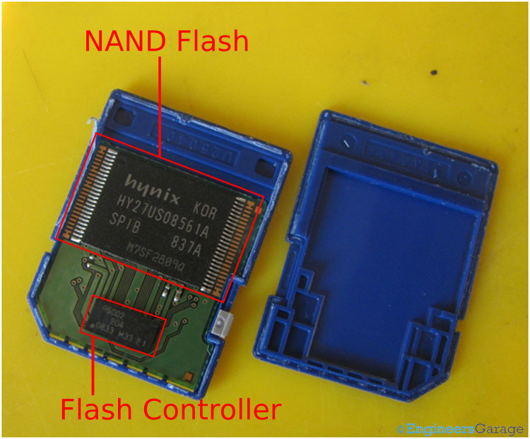
Internals of an SD card. Source: Engineers Garage
To read and write to the NAND chip, the host only needs to communicate with the flash controller, which will internally manage all interactions with the NAND chip. With this setup, the controller can contain algorithms to handle many of the complexities of using NAND flash without the host needing to do any additional work. Some of these include:
- Error correction code (ECC) handling
- Wear leveling
- NAND whitening
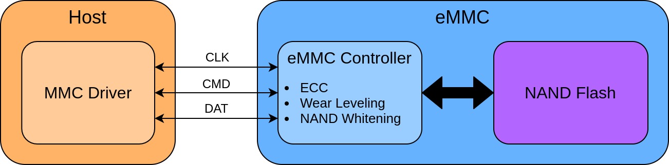
As the name implies, eMMC combines all of the components used for MMC into a single die and places it into a package that can be used in embedded devices, typically into a single ball grid array (BGA) chip. These chips will expose the same interface seen in MMC/SD cards, so a host will be able to follow the same protocol for communicating with them.
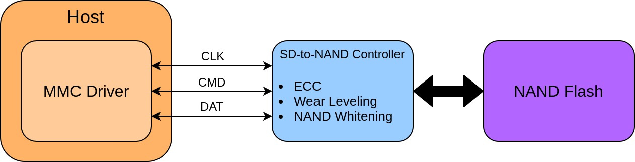
Some manufacturers opt to create a configuration that is essentially an SD card built into a larger board, consisting of a separate NAND flash chip and SD controller. As shown in the above diagrams, the interface for this setup is the same as a single eMMC chip, so everything detailed in this post will apply to these as well.
eMMC Bus Signals
The eMMC protocol is capable of operating in 1-bit, 4-bit, or 8-bit parallel I/O depending on the number of data lines being used. A command signal is used for initializing the eMMC chip and sending read/write commands. A single clock signal is used to synchronize all command and data lines, where they can be sampled on either the rising edge only, or both rising and falling edges for faster performance. These signals and additional pins are detailed in the table below:
eMMC Pinout Table
| Pin | Description |
|---|---|
| CLK | Clock line used to synchronize CMD and all DAT lines |
| CMD | Bidirectional line used for sending commands and responses to/from the chip. This is used during initialization to determine the number of data lines that should be enabled, the desired clock speed, and any other operating conditions. |
| DAT0 | Bidirectional data line, used in 1-bit, 4-bit, 8-bit modes |
| DAT1 | Bidirectional data line, used in 4-bit, 8-bit modes |
| DAT2 | Bidirectional data line, used in 4-bit, 8-bit modes |
| DAT3 | Bidirectional data line, used in 4-bit, 8-bit modes |
| DAT4 | Bidirectional data line, used in 8-bit mode |
| DAT5 | Bidirectional data line, used in 8-bit mode |
| DAT6 | Bidirectional data line, used in 8-bit mode |
| DAT7 | Bidirectional data line, used in 8-bit mode |
| VCC | Input voltage for flash storage, usually +3.3V |
| VCCQ | Input voltage for flash controller, usually +1.8V or +3.3V |
| VSS / VSSQ | GND for flash storage and flash controller |
Command Structure
The commands sent on the CMD line follow a fairly simple structure, and knowing how these look will help in identifying CMD in a logic trace. Commands are encoded in the following 48-bit structure:

| Name | Length (Bits) | Description |
|---|---|---|
| Start bit | 1 | Start of a command, always ‘0’ |
| Transmission bit | 1 | Indicates the direction of the command. 1: Host->Card 0: Card->Host |
| Command index | 6 | Value between 0-63 indicating the command type |
| Command argument | 32 | Value to be used by the command, e.g. an address |
| CRC | 7 | Checksum to validate the data was read correctly |
| End bit | 1 | End of a command, always ‘1’ |
Hands On
Now let’s take a look at a first generation Amazon Echo to show how to identify a pinout for an eMMC chip. Knowing this pinout, it may be possible to dump the contents of the chip without removing it from the PCB. However, in cases where that doesn’t work, we’ll cover a simple alternative once the chip is already lifted.
Here’s the device we’ll be working with:

Materials
The following materials are needed to follow along with this tutorial. You can pick these or other products that serve the same purpose. Links are included for your convenience (but note that we don’t endorse any of these vendors or products):
Needed to Follow Along
Needed for dumping lifted chip
Amazon Echo: Disassembly
The first step in taking apart the Amazon Echo starts at the bottom of the device. There’s a rubber cover lightly glued in place. Pulling up from the side is enough to pull it off.
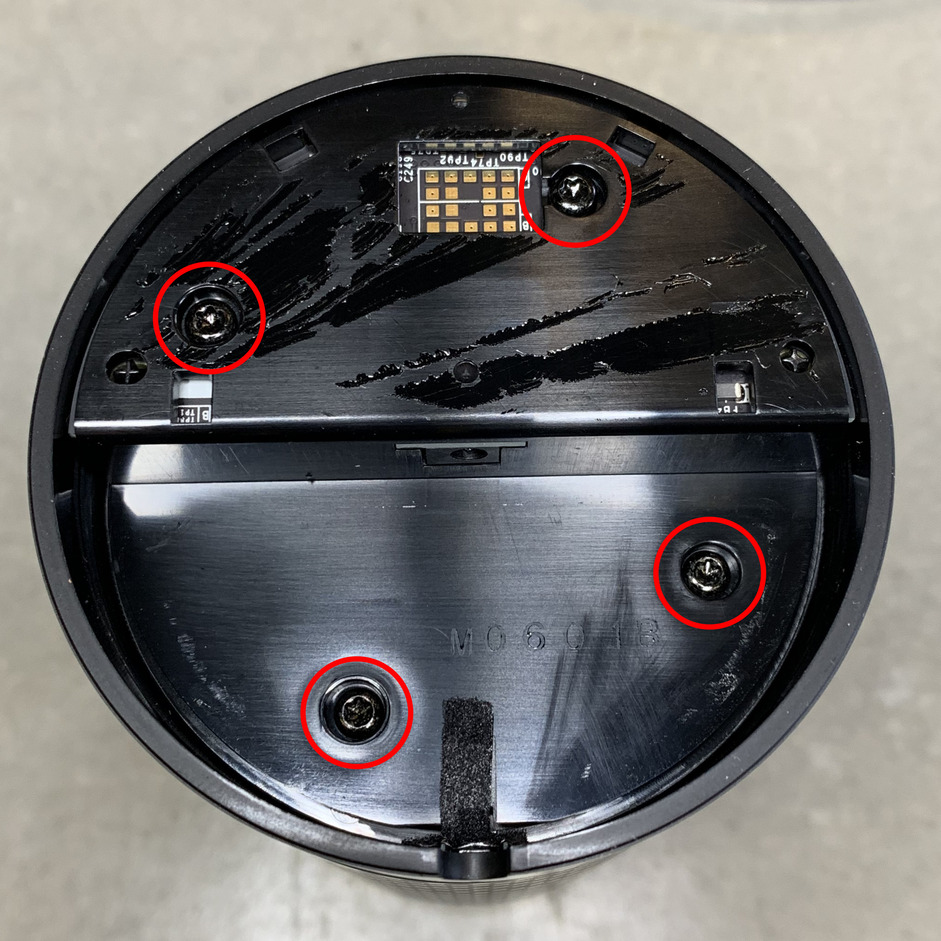
Next, there are 4 T10 screws that need to be removed in order to remove the bottom plate and access the first PCB.
Carefully lift the bottom plate out, and you’ll see speaker plugs and a ribbon cable still attached to the PCB. Pull the speaker plugs out, and disconnect the ribbon cable by lifting the dark brown lever away from the board.
Now the next plate covering the speaker can be lifted out. There are holes in this plate for the speaker cables and ribbon cable to pass through.
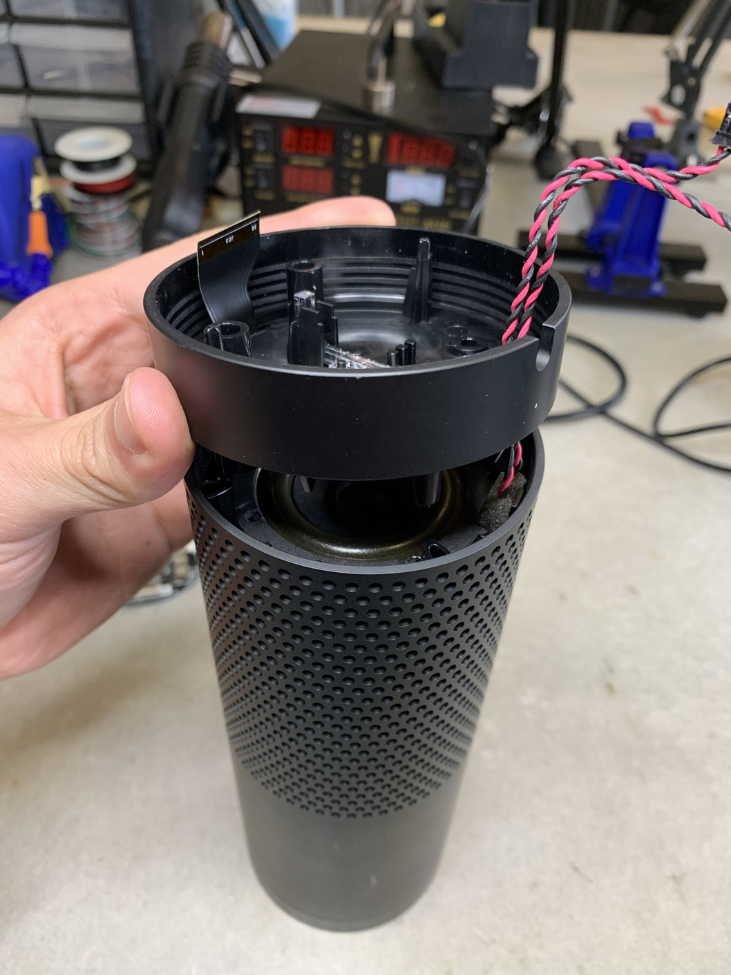
Then, the outer casing can be pulled off.
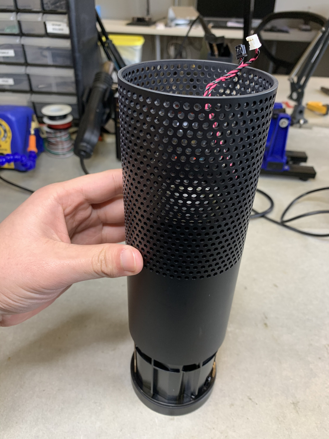
Next, peel off the felt paper wrapped around the device. There are a few glue strips holding it in place, so peeling these off the plastic as you go will allow the felt to come off cleanly.
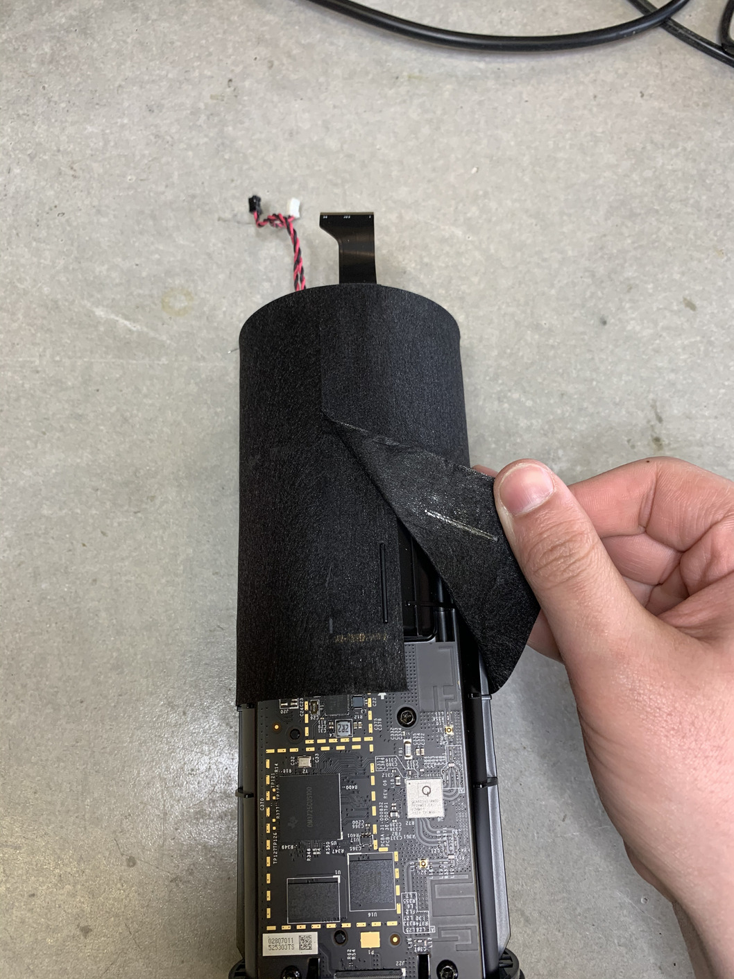
To remove the main PCB, there are 4 more T10 screws that need to be removed and 2 ribbon cables that need to be disconnected. The top cable (J21) is glued to the plastic with another glue strip. We’ll need this to power the main PCB later, so carefully peel off and remove the ribbon cable.
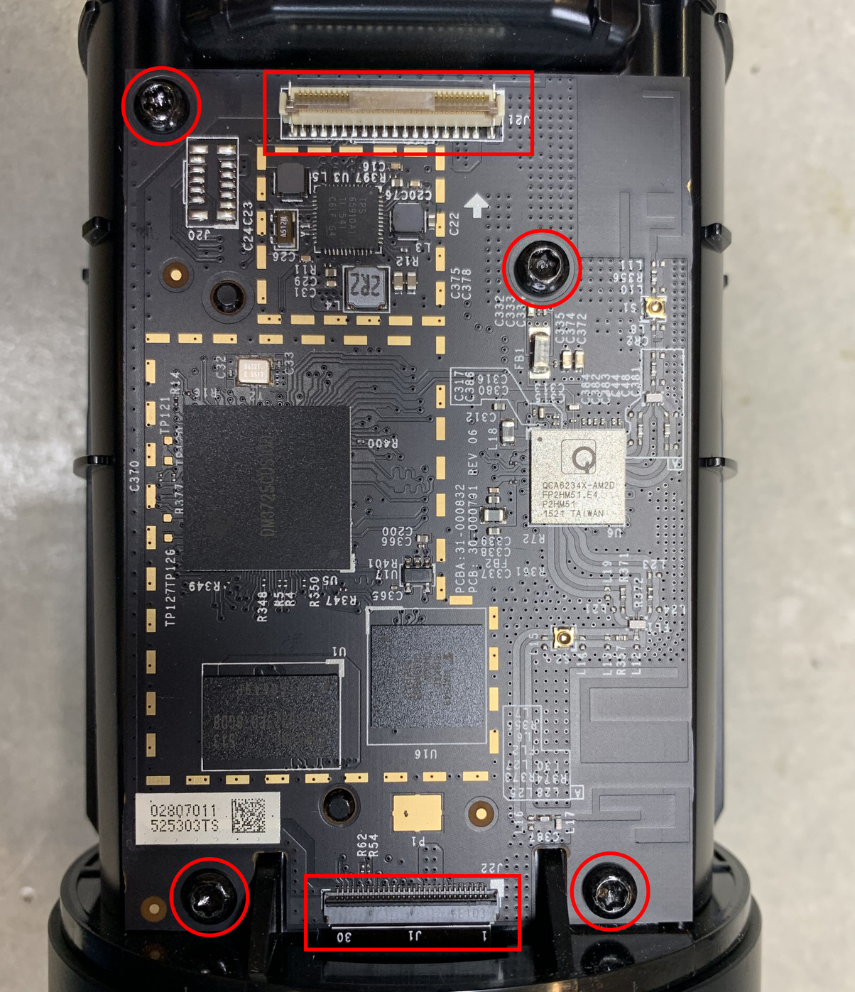
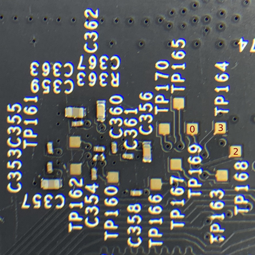
With the main PCB off, now we can take a look at all the components on it. These have been labeled in the image below:
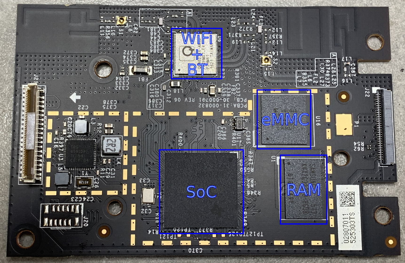
Amazon Echo: Logic Analyzer Setup
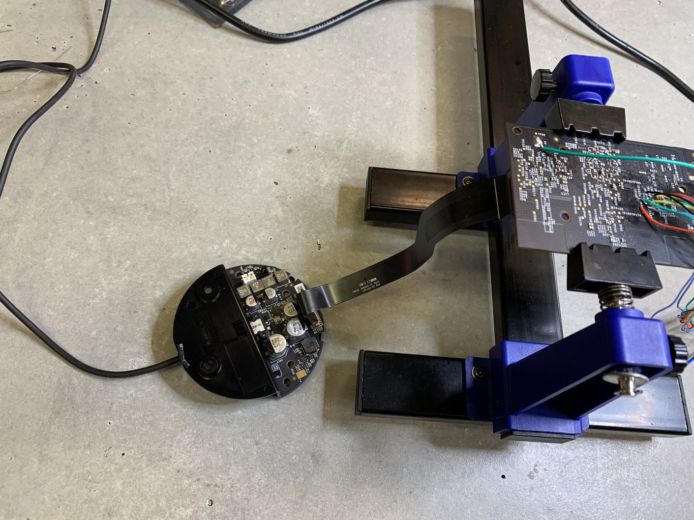
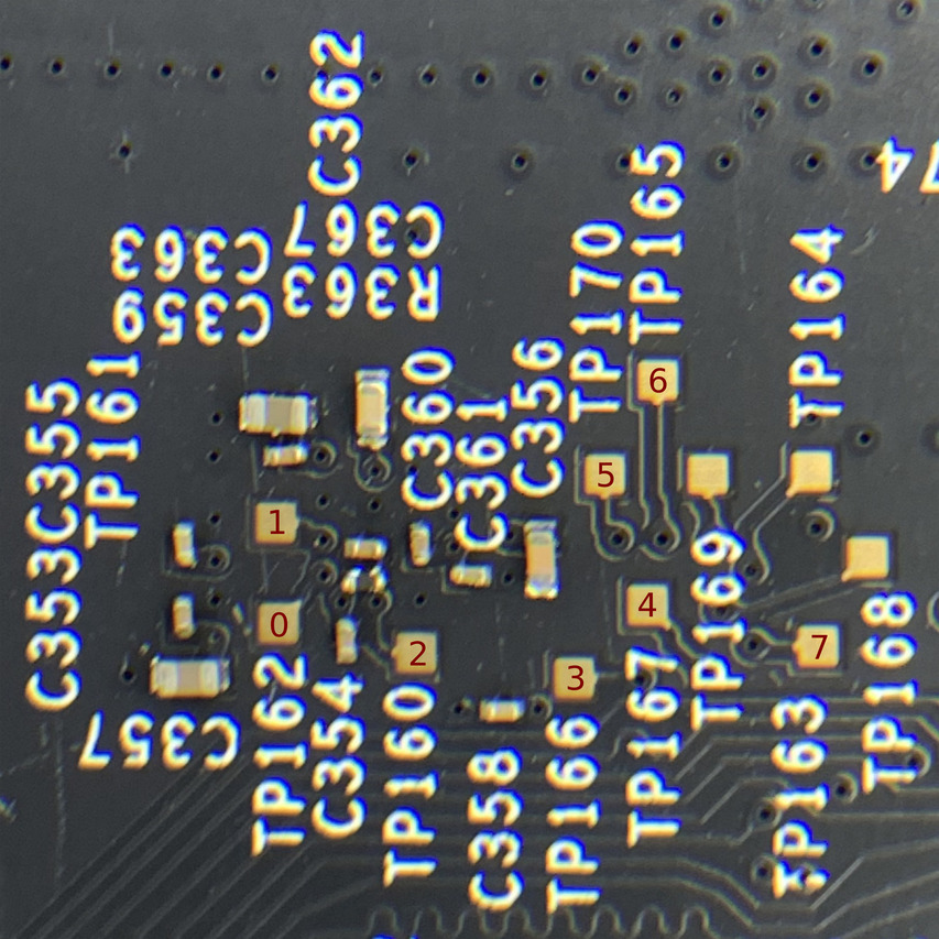
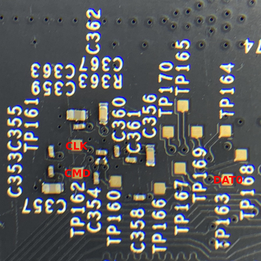
For now we only want to focus on the eMMC chip, which on this unit is a KIOXIA THGBMBG5D1KBAIT 4GB eMMC. Lucky for us, this board has as a number of test points on the other side of the board, directly opposite the eMMC chip.
The plan is to attach jumper wires to all of these pads and capture traces on the logic analyzer. From these, we should be able to identify a few of the main pins necessary to read an eMMC chip. The bare minimum we need is 3 pins to operate in 1-bit mode: CMD, CLK, and DAT0, along with a way to power the chip.
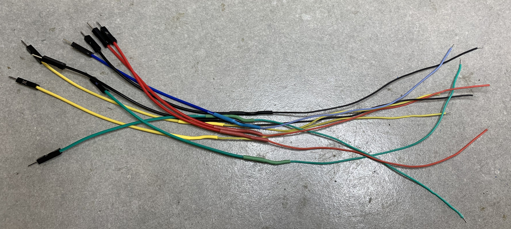
For this, I made some jumper wires with 30awg wire. Having a thin gauge wire like this is always very useful when soldering to any small components or pads like the ones on this board. Solder them all to the pads so we can take logic analyzer captures.
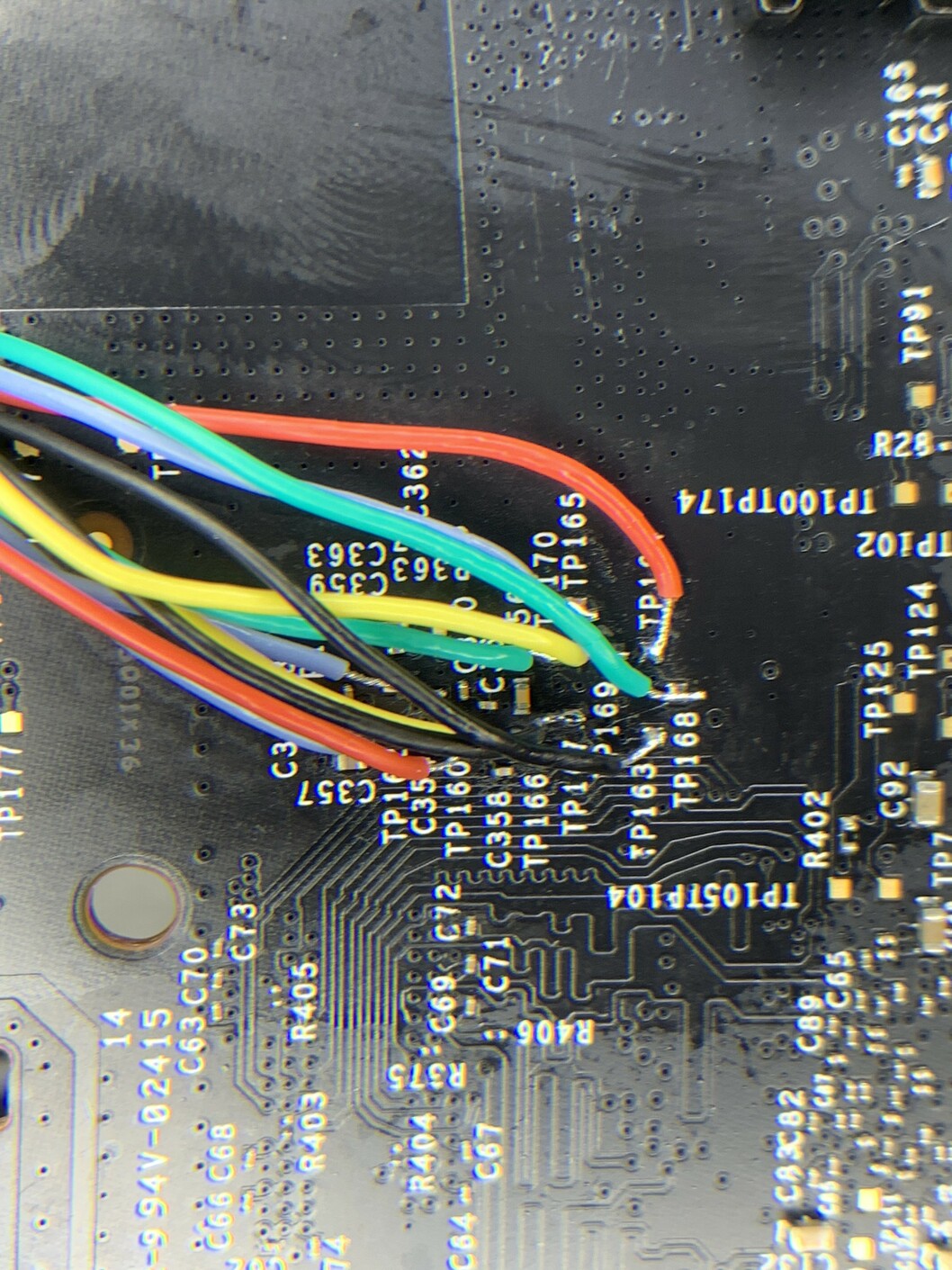
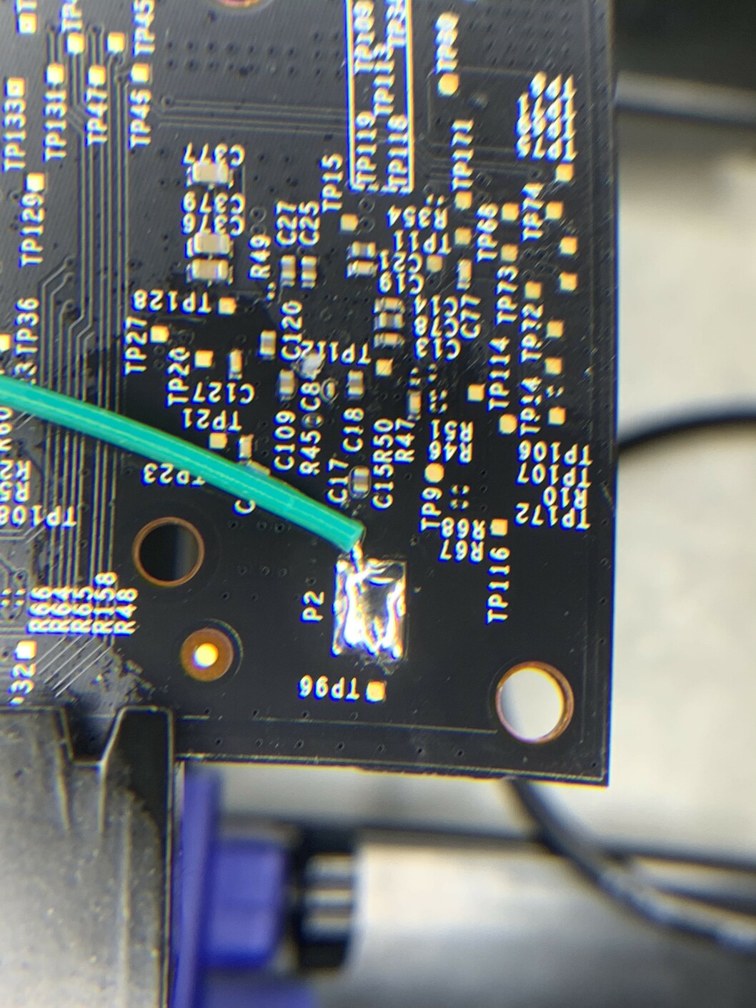
We also need a ground reference for the logic analyzer. On the same side of the board, the copper pad at P2 can be used for this. You can confirm this is ground by checking continuity between this and the shielding pads on the other side (the “dashed lines” of pads surrounding the chips).
To power the board, we need the ribbon cable and bottom plate of the echo we removed earlier. We can connect all of these together and plug in the power supply, and that will power the main PCB so we can capture traces. Here’s what the setup should look like:
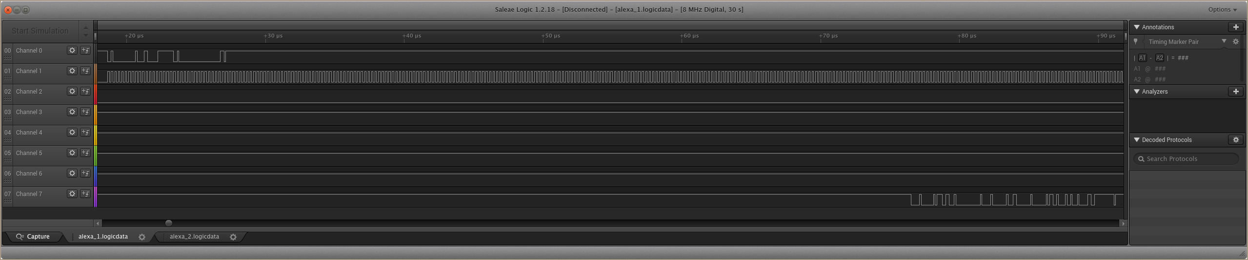
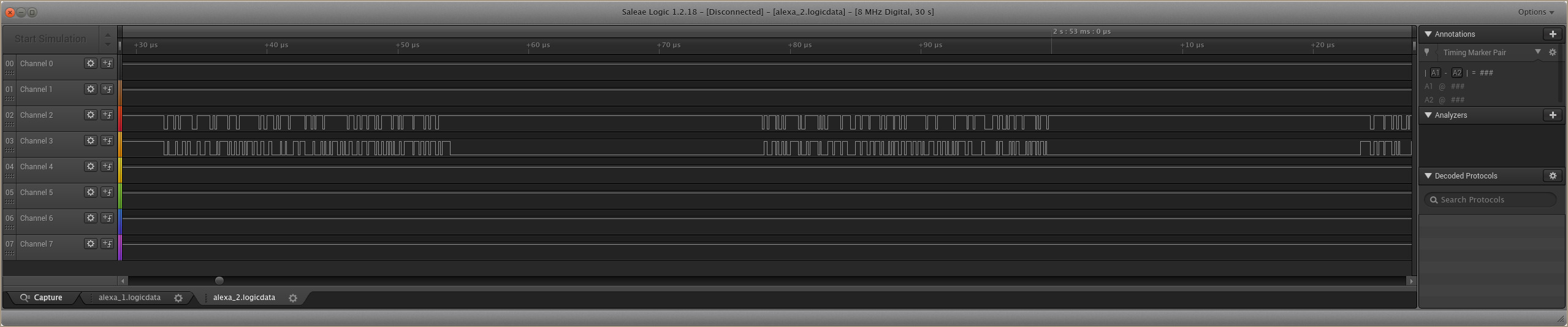
You’ll need more than one capture to account for all the pads being tested here. In each case, start a capture and power on the device, and you should see traces similar to the images below:
Capture 1
Capture 2
NOTE: Pin 1 is not connected
Trace Breakdown: Identifying Pins
It turns out that the first capture here has all the pins that we’re interested in. The first, and most obvious, is the CLK pin. This is Channel 1 in the example trace above, easy to identify by its fixed rate oscillation.
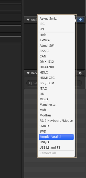
Next, we can try to identify CMD. This will be a line that’s active along with the CLK, and follows the structure covered above. We can use the Logic software to help identify this by adding an analyzer for parallel I/O. This is the “Simple Parallel” option:
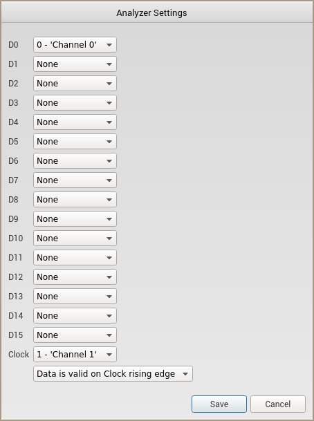
In the next menu, set the clock to the channel we already identified as CLK (Channel 1), and set D0 to a channel we want to analyze further. In this case, let’s look at ‘Channel 0’. Set all the other channels to ‘None’ (Tab + N is your friend here) and click ‘Save’.
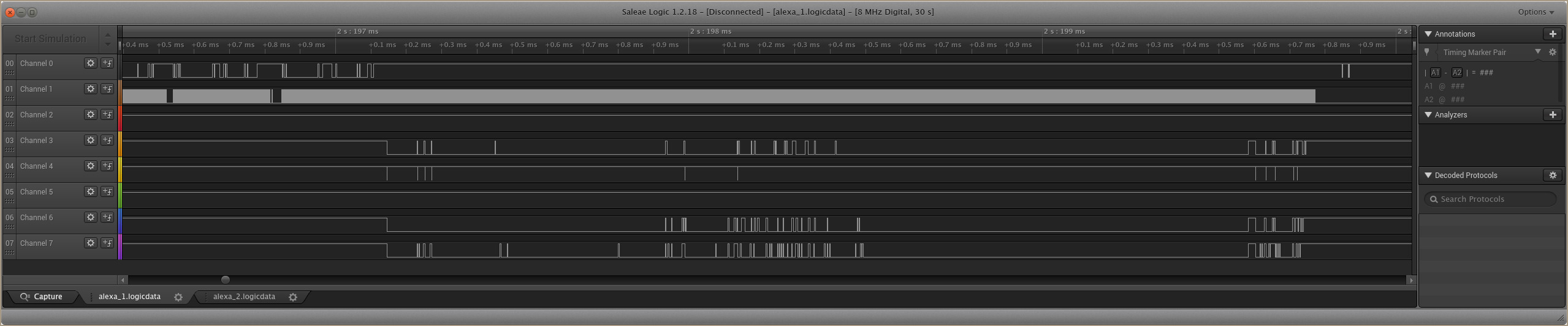
Now if you zoom in at a point where both channels are showing activity, the analyzer we just added will show the parsed binary values found by sampling all the rising edges on the clock. Here is an example Host->Card command:
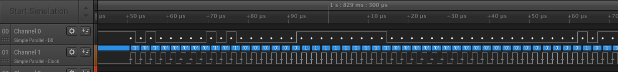
Followed immediately by a Card->Host response:

You can match both of these commands up with the structure we covered before.
-
In the first image, we see a start bit, 0, followed by 1 to indicate this is a Host->Card command, and the last bit is a 1.
-
The second image starts with 0, 0, indicating this is a Card->Host response, and once again ends in a 1.
We can see many commands following this same structure throughout the capture, so we can be fairly confident this is the CMD line.
Finally, we want to identify the DAT0 line. When initializing an eMMC chip, DAT0 is the only active data line since every host is capable of 1-bit communication. During the initialization phase the host and card will agree on the total number of data lines to be used, but by default it is always only 1. So, all we need to do is go to the beginning of the capture and see which data line shows activity first after CLK and CMD start up.
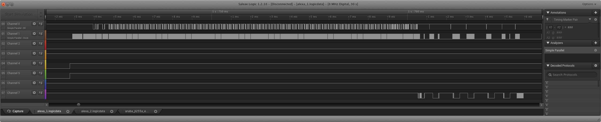
Here we can clearly see that after the first series of commands are sent, Channel 7 is the first to respond, so this likely DAT0.
Now looking back at the board, you should have identified the following pinout:
“Alexa, give me a flash dump”
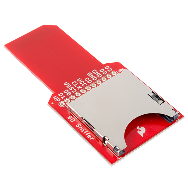
Depending on the device you’re working with, it may be possible at this point to dump the eMMC flash just by connecting to the pins that have been identified. Since this is the same MMC protocol used by SD cards, there are various adapters that can be used to connect to these pins and read them with any SD card reader. There are some pre-made examples, such as this Sparkfun SD Sniffer, where you can solder headers to the board and connect the pins to them directly.
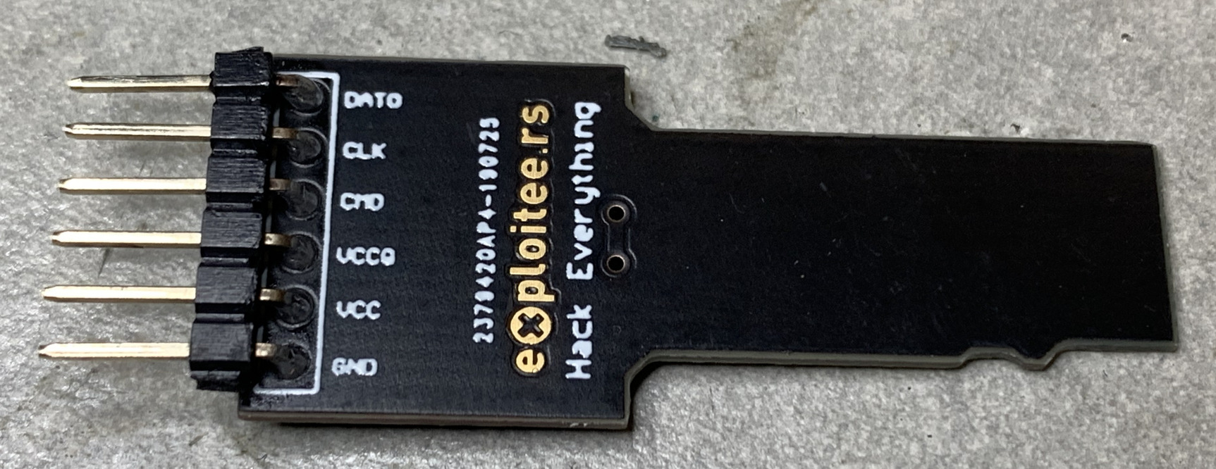
There’s also a similar microSD version made by exploitee.rs that only uses one data pin:
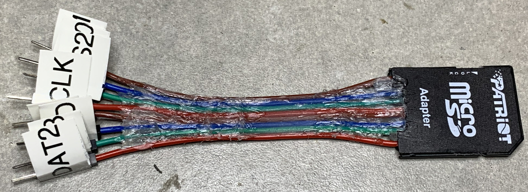
If you don’t have any of these but have a microSD to SD adapter, you can even turn that into a reader by breaking out all the pins inside:
Attempting to dump the chip while on the board may run into a few common issues. When powering on the board normally, the CPU is going to initialize and access the eMMC chip. Attempting to read the chip on another computer while this is happening will likely result in failing to detect it at all. One option around this is to try preventing the CPU from going through it’s normal boot process. For example, if you’re working on a device where the CPU uses a bootloader on a separate SPI flash, you can manually deselect the SPI by pulling its CS pin high or low (depending on the chip). This leaves the eMMC powered on but untouched by the CPU.
Another option is to try powering the eMMC chip externally when you try reading it. However, attempting to do this could result in other devices getting powered, such as the CPU, which results in the same issues as before. In the case of this test device, I wasn’t able to get it reading while still on the board, so now we’ll look into how to dump it by lifting it off the board.
Lifting & Reading the Chip
The first step is of course to lift the eMMC chip off the board. The easiest way to do this is using either a hot air station, or an infrared rework station. Here’s a simple tutorial on how to do this with hot air.
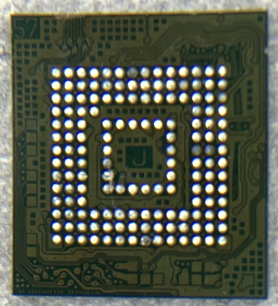
Once lifted, clean off all the remaining solder on the chip using solder wick. The chip should now look like this:
One of the easiest ways to read the chip is using an adapter, such as those from AllSocket. Most eMMC chips have a standard location for the pins needed for power and communication, so the socket breaks out these pins to an SD card you can plug it into a reader. To use this, simply place the chip inside the socket, aligning the dot on the chip with the arrow in the socket, and close it.
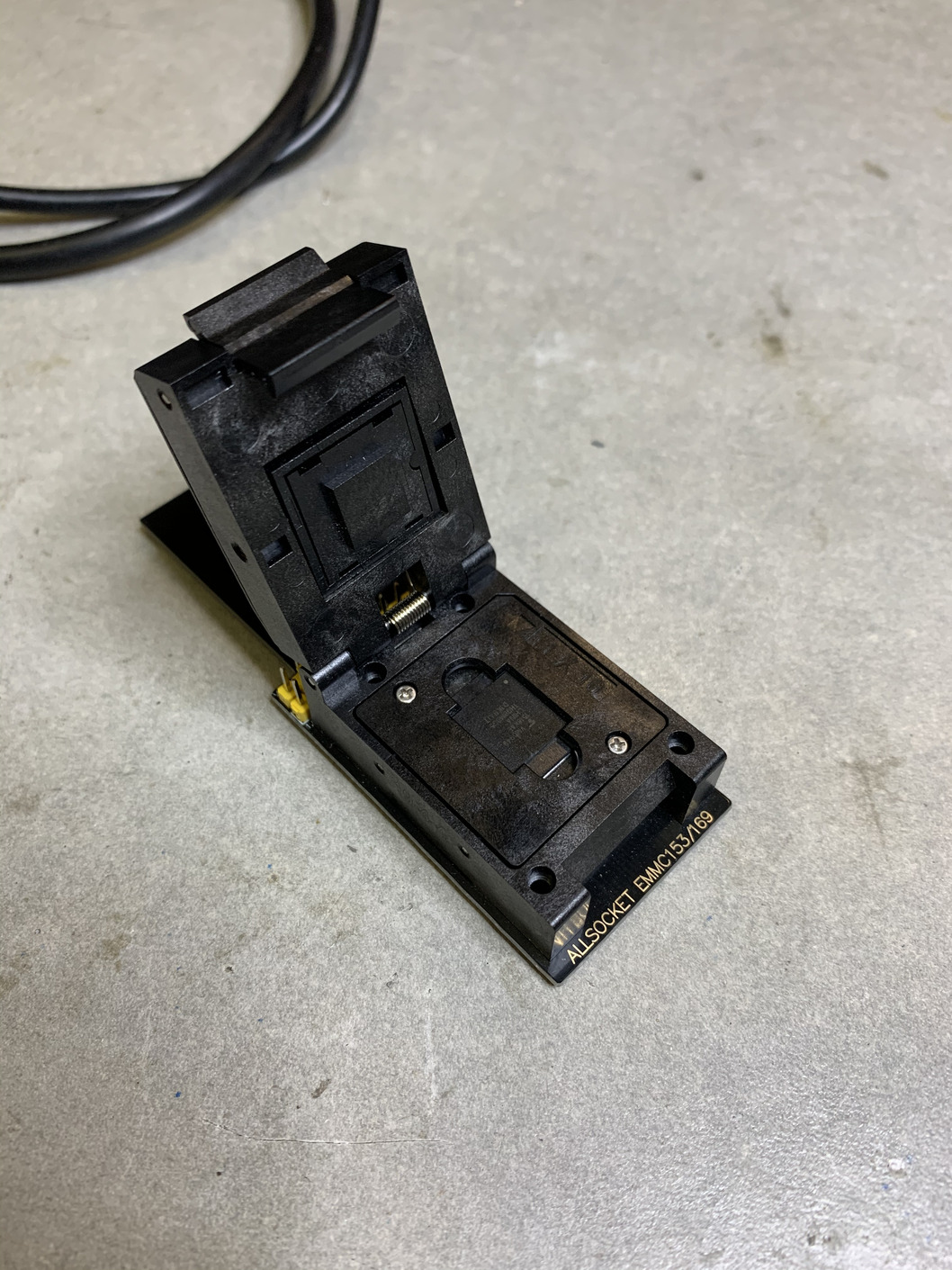
Then, plug the adapter into your laptop/SD card reader and it should detect and read the eMMC chip.
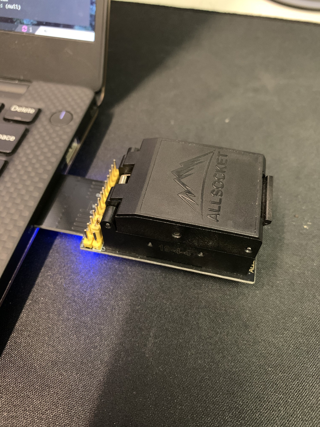
To check if your computer detected the chip correctly, run dmesg in
your terminal, and look for a snippet similar to this:
dmesg Output
[25103.832356] mmc0: new high speed MMC card at address 0001
[25103.833673] mmcblk0: mmc0:0001 004GE0 3.69 GiB
[25103.834188] mmcblk0boot0: mmc0:0001 004GE0 partition 1 2.00 MiB
[25103.834722] mmcblk0boot1: mmc0:0001 004GE0 partition 2 2.00 MiB
[25103.836965]  mmcblk0: p1 p2 p3 p4 p5 p6 p7 p8
[25104.636138] EXT4-fs (mmcblk0p4): mounting ext3 file system using the ext4 subsystem
[25104.637872] EXT4-fs (mmcblk0p4): warning: maximal mount count reached, running e2fsck is recommended
[25104.638357] EXT4-fs (mmcblk0p4): mounted filesystem with ordered data mode. Opts: (null)
[25104.901046] EXT4-fs (mmcblk0p7): mounting ext3 file system using the ext4 subsystem
[25104.910998] EXT4-fs (mmcblk0p7): mounted filesystem with ordered data mode. Opts: (null)
[25105.165884] EXT4-fs (mmcblk0p5): mounting ext3 file system using the ext4 subsystem
[25105.171570] EXT4-fs (mmcblk0p5): mounted filesystem with ordered data mode. Opts: (null)
[25105.411127] EXT4-fs (mmcblk0p6): mounting ext3 file system using the ext4 subsystem
[25105.420283] EXT4-fs (mmcblk0p6): mounted filesystem with ordered data mode. Opts: (null)
[25105.667704] EXT4-fs (mmcblk0p8): mounting ext3 file system using the ext4 subsystem
[25105.677490] EXT4-fs (mmcblk0p8): mounted filesystem with ordered data mode. Opts: (null)
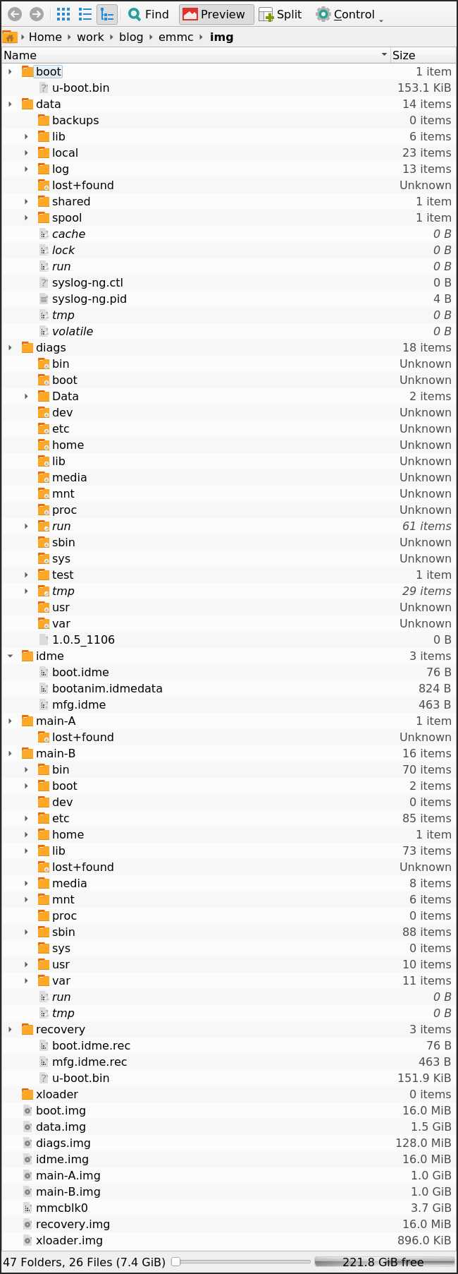
Mounted Partitions
$ lsblk
NAME          MAJ:MIN RM   SIZE RO TYPE  MOUNTPOINT
mmcblk0       179:0    0   3.7G  0 disk
├─mmcblk0p1   179:1    0   896K  0 part
├─mmcblk0p2   179:2    0    16M  0 part  /mnt/mmcblk0p2-mmc-004GE0_0xf01af56
├─mmcblk0p3   179:3    0    16M  0 part  /mnt/mmcblk0p3-mmc-004GE0_0xf01af56
├─mmcblk0p4   179:4    0    16M  0 part  /mnt/mmcblk0p4-mmc-004GE0_0xf01af56
├─mmcblk0p5   179:5    0   128M  0 part  /mnt/mmcblk0p5-mmc-004GE0_0xf01af56
├─mmcblk0p6   179:6    0     1G  0 part  /mnt/mmcblk0p6-mmc-004GE0_0xf01af56
├─mmcblk0p7   179:7    0     1G  0 part  /mnt/mmcblk0p7-mmc-004GE0_0xf01af56
└─mmcblk0p8   179:8    0   1.5G  0 part  /mnt/data
mmcblk0boot0  179:256  0     2M  1 disk
mmcblk0boot1  179:512  0     2M  1 disk
It’s that easy! Now we can save a full image of the chip and extract all the partitions from there:
$ sudo dd if=/dev/mmcblk0 of=mmcblk0 status=progress bs=16M
3959422976 bytes (4.0 GB, 3.7 GiB) copied, 165 s, 24.1 MB/s
236+0 records in
236+0 records out
3959422976 bytes (4.0 GB, 3.7 GiB) copied, 164.523 s, 24.1 MB/s

$ 7z x mmcblk0
Scanning the drive for archives:
1 file, 3959422976 bytes (3776 MiB)

Extracting archive: mmcblk0
--
Path = mmcblk0
Type = GPT
Physical Size = 3959422976
ID = F9F21FFF-A8D4-5F0E-9746-594869AEC34E

Everything is Ok

Files: 8
Size:       3959274496
Compressed: 3959422976

$ ls -lh
total 7.4G
-rw-r--r-- 1 user  user   16M Mar  3 18:17 boot.img
-rw-r--r-- 1 user  user  1.6G Mar  3 18:17 data.img
-rw-r--r-- 1 user  user  128M Mar  3 18:17 diags.img
-rw-r--r-- 1 user  user   16M Mar  3 18:17 idme.img
-rw-r--r-- 1 user  user  1.0G Mar  3 18:17 main-A.img
-rw-r--r-- 1 user  user  1.0G Mar  3 18:17 main-B.img
-rw-r--r-- 1 root  root  3.7G Mar  3 18:17 mmcblk0
-rw-r--r-- 1 user  user   16M Mar  3 18:17 recovery.img
-rw-r--r-- 1 user  user  896K Mar  3 18:17 xloader.img
Most of these are regular filesystems that can be mounted, so let’s mount them all so we can see what they contain:
$ for i in *.img; do
NAME=$(basename "$i" .img)
mkdir "$NAME"
sudo mount "$i" "$NAME"
done
Just like that, we now have full dump of the Echo’s firmware!
Conclusion
These are all the basics of how to look for eMMC signals on a board, and how to go about reading these chips. The example device used here conveniently had pads for all of the eMMC pins, but this isn’t always the case. Using what you’ve learned here, you can try capturing traces at any components, such as resistors near an eMMC chip to find an alternate pinout.
With the Echo’s firmware dumped, we can start analyzing all the services running on the device searching for vulnerabilities, as well as look into the data stored on the device.
For more details about eMMC, the full standard can be found on JEDEC’s website.
In our next post in the Hardware Hacking 101 series, we’ll be covering ISP. Keep an eye out for it, and contact us at any time with questions or to discuss how we can help with your product security needs!
UPDATE: Thanks to @m33x, we’ve been made aware of Clinton, Cook, et al’s paper which mentions an “eMMC Root” as a possible method in Section IV.A, although that work doesn’t apply or test the method. Also, he mentions Alexa, Are you Listening? which is using debug pads to mount/boot from an external SD card, which is different than what this article shows.